Foreword
In the previous post we managed to integrate our VIC-II module with our c64 core and completed a successful simulation where our VIC-II core rendered the pixels of an image of the C64 Welcome screen.Well, I see that it is about a month ago since I wrote my previous post and the reason for that is that I have been hitting a kind of a brick wall trying to implement the c64 core with the VIC-II module on the physical FPGA.
The major issue I was experiencing was using Block RAM in Dual port mode. The basic idea was that the 6502 access the main 64KB memory via the one port and the VIC-II core access the same RAM via another port.
However, when running the design on the FPGA, it was only the 6502 core that could retrieve sensible data from the Block RAM. The VIC-II only got a single value all the time: A hex FF.
I eventually resolved above mentioned issue by eventually resolving to trial and error.
In this post I will elaborate a bit more on the problem, plus some steps I followed in trying to resolve the issue.
In doing some research in trying to solve the Dual Port Block RAM issue, I also came across some resources talking about dealing with multiple clocks in an FPGA design.
My current design do have a couple of different clock speeds: 8MHz, 2MHz and 1Mhz. I am however not dealing with them in quite the right way as discussed in the above mentioned resources.
So, in this post I will also cover a bit of the detail on how I change the way I handle the different clocks in my design.
The Problem and Initial Analysis
So, I managed to load the implementation of the combined 6502 and VIC-II design to the FPGA as well as managing to write an output frame of the VIC-II to the SDRAM of the Zybo board.Next step obviously was to download the frame data from the SDRAM of the Zybo to my PC as a binary file and converting it to a ppm image file so I can view it in an image editor.
The resulting image was somewhat disappointing:

No C64 welcome message, but some kind of checker pattern!
Eventually I could narrow it down that the VIC-II module is ready the character code xFF from screen memory repeatedly:

By using an Integrated Logic Analyser I confirmed that the Block RAM port connected to the VIC-II is indeed only returning the code xFF. Integrated Logic Analysers is a useful tool for performing debugging on the FPGA itself which I will cover in a coming section.
I did a bit of reading on the Internet on the issue and I had some suspicion that the issue was caused by the way I handle clocks in my design.
So, I go about making lots of changes to my design in the way I handle clocks. Sadly, though, none of these changes exchanged the checker screen for the C64 welcome screen.
A bit of light at the End of the tunnel
My Checker screen problem kept me busy for more than a month.At one stage I even suspected that the Zynq chip on my Zybo board was part of a faulty batch in that only port of the Block RAM works.
I just couldn't explain why the one port could give sensible data for the 6502 system and not on the other port for the VIC-II. What could be different?
In the back of the head, though, I new about a significant difference: The 6502 accessed almost the complete range of the 64KB RAM whereas the VIC-II only accessed the first 16KB (as done per design).
Could it be that a port on Block RAM should access the whole range of the 64KB as part of the initialisation process?
The Xilinx documentation for Block RAM didn't really give some supporting clues for my theory. However, no harm could be done for testing my theory.
To test my theory, I made the following changes to the 64KB block RAM of my C64 design:
...
    reg [7:0] ram [65535:0];
    reg [15:0] counter;
...
always @(posedge clk_2_mhz)
  counter <= counter + 1;

     always @ (posedge clk_1_mhz)
       begin
        if (we)
        begin
         ram[addr] <= ram_in;
         ram_out <= ram_in;
        end
        else
        begin
         ram_out <= ram[addr];
        end
       end

    always @ (posedge clk_2_mhz)
       begin
         ram_out_2 <= ram[counter];
       end
In effect we have added a counter counting from 0 to 655535 and use it as an address input to the second port of our Block RAM. In this way we exercise the full address range.
Inspecting ram_out_2 with a Logic Analyser after applying above change, does look promising. In the screen memory address range we see mostly the character code 20Hex (e.g. the space) and the character codes of the welcome message in the positions expected.
It does seem that iterating through the full range of memory does indeed make a difference!
Fixing the VIC-II design
Been able to get some sensible data from both ports of the 64KB Block RAM, let us see if we can proceed to fix our VIC-II design.The idea is continuously loop through all the contents of the 64KB Block RAM as done in the previous section for about two seconds. After the two seconds we remove the counter from the address input of the applicable port and connect the address output of our VIC-II module to that port.
This strategy boils down to the following changes:
    wire [15:0] portb_add;
    reg [24:0] portb_reset_counter = 0;
...
    assign portb_add = (portb_reset_counter < 3900000) ? portb_reset_counter[15:0] : {2'b0,vic_addr};
    reg [24:0] portb_reset_counter = 0;
...
    always @(posedge clk_2_mhz)
    if (portb_reset_counter < 4000000)
      portb_reset_counter <= portb_reset_counter + 1;
...
     always @ (posedge clk_1_mhz)
       begin
        if (we)
        begin
         ram[addr] <= ram_in;
         ram_out <= ram_in;
        end
        else
        begin
         ram_out <= ram[addr];
        end
       end

    always @ (posedge clk_2_mhz)
       begin
         ram_out_2 <= ram[portb_add];
       end
So, we basically define a counter counting to 4000000, which corresponds to 2 seconds with a 2MHz clock.
In the two seconds we use the lower 16 bits of the counter to give addresses in the range 0 to 65535 to the applicable port.
Just before the two seconds is over, we connect the address output of our VIC-II module to this port.
Running the design on the FPGA and doing a quick inspection with a ILA confirmed that we are more or less on track:

The first row is the address output of our 6502.
The third row is the address output of our VIC-II module. Directly below this is the data output from our Block RAM for given addresses.
The row at the bottom is the 2 MHZ clock signal driving our VIC-II. It looks a bit different from what we have seen from previous posts, but more on this later.
Debugging with an Integrated Logic Analyser
In previous sections I mentioned the use of Integrated Logic Analysers (ILA). In this section I will describe how to use them.An Integrated Logic Analyser is almost like an oscilloscope allowing you to inspect the signal of a wire or a register within your design.
I will start this section by describing how to add a ILA to your design.
You can add add an ILA within your Block Design editor. So, with your block design open, click the Add IP button and within the search box type ILA:

The component we are after is the first one shown, ILA (Integrated Logic Analyser). So double click on this item.
An ILA will be added to your design as shown below:

We will, however, need to configure the instantiated ILA component before it can be useful for us, so double click on it.
We need to change the Monitor type to Native. With native selected as the Monitor type, the configuration window will look as follows:

In the Probe Ports tab you need to specify the probes the size of probes that are more than one bit wide. Typically this tab will look something like the following when configured:

With the ILA configured you can hit the OK button and you will see the ILA block in your design been modified accordingly.
What remains to be done is to link up the wires to be probed:

Just a note on the clk pin of the ILA block. It is important that pin should be connected to the input clock source of the FPGA. On the Zybo board, for instance, the frequency on this clock source is 100Mhz.
With the ILA been added and wired up in your design, you kick off the synthesise design process. With the Synthesise process finished, there is a couple of additional steps you should do.
Firstly you need to open the synthesised design and drill down in the schematic till you see the ILA component.
You will see each of the signals you have defined as a probed is marked with a "bug" icon. You should now control-select all these signals. This will look something like the following:

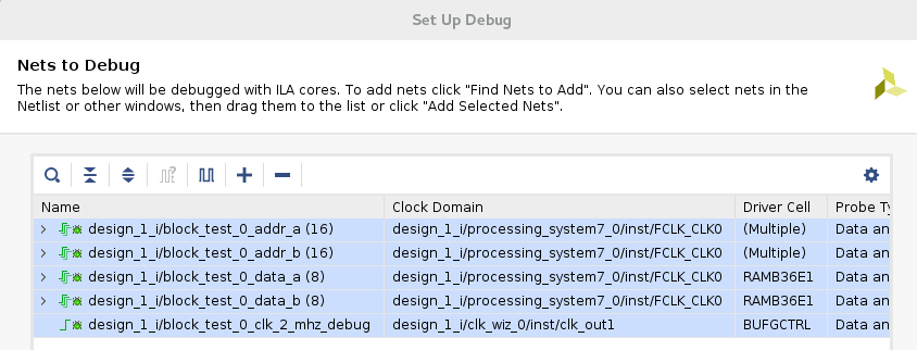
With these signals selected, open up the Debug Window and then click the Setup Debug button. A wizard will open. Continue clicking next.
On the Nets to Debug page ensure all the lines are highlighted:
On the next page you need to select a sample depth. I always specify a value of 2048. This page in effect you specify how many samples you want to capture and display at a time.
It should be noted that an ILA makes use of the Block RAM resources on your FPGA to store the captured samples. So the more signals you want to capture and the bigger the required data depth, the less Block RAM resources you will have available for your design.
With the data depth specified, keep clicking Next till the Wizard closes. When the Wizard closes, Vivado will make some small changes to the schematic looking something like the following:

It is at this point where we can inspect some signals with the ILA.
We will be inspecting the signals in Vivado while our app is running via Xilinx SDK. So, within Vivado click Open Hardware Manager and then do a open connect. You will then be presented with a waveform window at which you can the signals you want to inspect. You are now ready to view some signal data:
To see the signals immediately you can just hit the double arrow button in the toolbar.
In our c64 core, hitting the double arrow you will see a space char (0x20) most of the time for the signal data_b(e.g. data out to the VIC-II) core.
To see part of the signal where we expect part of the welcome message, the trigger immediate would not be that useful.
This is where the Trigger on Condition comes in handy where you specify a condition that should be met before starting capturing samples.
To trigger on a condition, you first need to setup a condition. You do this by pressing the plus(+) button in the Trigger Setup panel (bottom right).
An example of a trigger been setup is shown below:

In this example a conditional trigger would only start capturing samples if addr_b encounters value 432Hex. This would fit our needs of showing part of the signal where we expect part of the welcome message.
The conditional trigger is started by pressing the play button in the toolbar.
On clock domains in the design
As mentioned earlier on, I changed the way a bit I handle multiple clocks in my design in attempt to align with best practices.Our c64 design makes use of three clock frequencies: 8MHz, 2Mhz and 1Mhz.
The 2MHz and 1MHz frequencies both derived from 8MHz via a frequency divider which is a counter of which the 2Mhz is retrieved via bit 1 and the 1Mhz frequency via bit 2 of the counter.
In the design described previously I linked the parts of the circuit clocking on 1Mhz and 2Mhz directly to the bits mentioned above.
This approach is prone to clock skew and can cause erratic clock spikes.
Clock domains in an FPGA is quite a big topic to research, but the following post in Xilinx forum gave me a head start: https://forums.xilinx.com/t5/7-Series-FPGAs/How-to-divide-a-clock-by-2-with-a-simple-primitive-without-Clock/td-p/783488
The following diagram mentioned in the forum post gave me an idea what to do:

The left side of the circuit receives a clock input, which in our case would be the 8MHz generated clock.
On the top the clock signal gets passed through a BUFG primitive. This is a buffer living in the global clock domain within the FPGA fabric. This buffer has a high fan out an minimise clock skew.
From the output of BUFG we drive a clock divider in turn drives the enable pin of a BUFGCE component.
In our design we will have two BUFGCE instances. The first instance will only enable every eighth pulse of the 8MHz signal to get a 1 MHz signal. Of course the resulting signal will not have a 50% duty cycle.
Similarly we will have a second BUFGCE instance enabling every fourth pulse of the 8Mhz signal to get a 2Mhz signal.
To incorporate these changes, I did the following:
...
    reg [2:0] clk_div_counter = 0;
    reg clk_1_enable;
    reg clk_2_enable;
...

    always @(negedge clk)
      clk_1_enable <= (clk_div_counter == 7);

    always @(negedge clk)
      clk_2_enable <= (clk_div_counter == 2) | (clk_div_counter == 6) ;

    always @(posedge clk)
      clk_div_counter <= clk_div_counter + 1;

       BUFGCE BUFGCE_1_mhz (
       .O(clk_1_mhz),   // 1-bit output: Clock output
       .CE(clk_1_enable), // 1-bit input: Clock enable input for I0
       .I(clk)    // 1-bit input: Primary clock
    );

       BUFGCE BUFGCE_2_mhz (
       .O(clk_2_mhz),   // 1-bit output: Clock output
       .CE(clk_2_enable), // 1-bit input: Clock enable input for I0
       .I(clk)    // 1-bit input: Primary clock
    );
...
You might be wondering why I didn't include an instance of BUFG in my code. The reason is that the Clock Wizard I used to create the 8MHz clock already added a BUFG instance in the path.
The final thing we should do with our clocks is constraining it.
Constraining is a widely used term in FPGA tools. Within FPGA tools you can constrain many things and clocks is one of them. When you constrain a clock in an FPGA tool, you are basically giving information about one or more clocks to the tool, like frequency, duty cycle and so on.
The FPGA tool then uses this information while performing the synthesis in order to create an optimum design and try to meet timing constraints posed by the frequency.
These clock constraints you need to add to a constraint file, which you can locate in the source tree as follows:

create_generated_clock -name clkdiv1 \
   -source [get_pins design_1_i/block_test_0/inst/BUFGCE_1_mhz/I0] \
   -edges {1 2 17} [get_pins design_1_i/block_test_0/inst/BUFGCE_1_mhz/O]

create_generated_clock -name clkdiv2 \
   -source [get_pins design_1_i/block_test_0/inst/BUFGCE_2_mhz/I0] \
  -edges {7 8 15} [get_pins design_1_i/block_test_0/inst/BUFGCE_2_mhz/O]
For both clocks we specify the input pin of the applicable BUFGCE instance as the clock source. These names can be found via the Synthesised design schematic.
Similarly each constraint ends with name of the output pin of the BUFGCE as the destination clock.
The -edges option may look a bit confusing. Basically you define the shape of the destination clock signal in terms of the source clock.
You start by taking your source clock and numbering all its edges starting at one. You then specify the target clock using these edges. The three numbers in curly brackets represents the rising first rising edge of the destination clock, falling edge and the next rising edge.
The following diagram will clarify these parameters a bit:

The top graph represents the source clock with all edges numbered.
The centre graph is our 1MHz signal. It starts at source edge 1 and falls at source edge 2. It repeats at source edge 17.
Similarly we have our 2MHZ as the bottom graph. It starts at source edge 7 and falls on source edge 8 and repeats on source edge 15.
That is it concerning the clock domains for our design.
In Summary
In this post I have covered the issues I experienced the issues I had in using a Block RAM in dual port port mode and how I got around it.I also explained how to use Integrated Logic Analysers to inspect one or signals while your design is running on the FPGA.
I ended off the post by explaining how to properly constrain the clocks I used in the design.
In the next post I we continue getting our design to write the frame output of our VIC-II core to SDRAM.
Till next time!