Thursday 24 March 2022

Read Levelling on the Arty A7

Foreword

In the previous post we had a look at write levelling. Write levelling is required on DDR3 because control signals to different memory chips are daisy chained. This means that the control signals travel different distances to different memory chips, which at high frequencies can lead to significant clock skew.

In DDR3 we try to compensate for this clock skew, by delaying the data strobe signal for each byte lane by a specific amount during reading and writing.

The process of determining the amount of delay required for the strobe signals is called write levelling and read levelling.

In this post we will be covering read levelling, still basing our design heavily on the Elphel Memory controller of the 10393.

Simplifying the plot

The more I read about read and write-levelling, the more I am convinced that it is a bit of a overkill to run these processes every time when you power up an Arty A7.

As I mentioned previously, these levelling processes is to account for the difference in distances the control signals need to travel to different memory chips.

However, the Arty A7 contains just one memory chip, and not several. With just that assumption alone, one doesn't need to worry about clock skew among different memory chips.

One might also argue, even though we only have one memory chip, it can be potentially far away from the FPGA, also causing annoying clock skew, which we need to correct with the levelling processes.

Looking at the layout of the Arty A7, we see that this is again not the case:


I got this image from Digilent's web site. Item number 19 is the FPGA and item number 20 is the RAM chip. Measuring the distance between the two components is about 1 centimetre. This distance is almost nothing compared to the distance between CPU's and RAM on other motherboards.

Also, I am clocking RAM at 333MHz, so if you strobe the data at a quarter of a clock cycle after the data was asserted, this would be more than enough to counter any clock skew due to the distance between the FPGA and the RAM chip.

From all my measurements so far, I also found that I could reliably read data from the RAM chip when I use a quarter cycle delay before doing the strobe.

If this assumption remains valid throughout my project, this will simplify my design greatly, in the sense that I don't need to add logic for running levelling upon powerup.

Having said that, putting the RAM chips in write levelling or read levelling mode is still useful for doing research, like this post.

Using the ISERDESE2 and OSERDESE2 blocks

I mentioned in the previous section that on the Arty A7 that the RAM chips are clocked at 333MHz. However, the FPGA on the Arty A7 is not able function properly at such high frequencies, so how do we solve this?

Most of you will know that this kind of problem is not a new one in the Computer world. Just think of the reason why most Disk Drives produced for the Vic-20 and Commodore 64 were so slow, compared to Disk Drives for other computers of the era.

Starting with the Vic-20, they replaced the parallel Disk interface, which was used in the PET's, with a serial one, meaning that this new port had to be clocked theoretically at 8 times the clock speed to get the same performance as a Disk Drive of the Pet. They intended to use the serial shift register on the 6522 to reduce the load on the CPU.

We all now the rest of the story. They couldn't use the shift register of the 6522, because it had a bug, so they had to resolve to bit banging, which is the reason for the slow Disk load speeds. The CPU is simply not powerful enough to provide the same throughput of a parallel port, in serial bit banging fashion.

To come back to our Arty A7 that cannot operate at 333MHz. We can also solve this issue with a serial shift register, but we will need a shift register for every bit of info between the memory chip and the FPGA. This will become clear in a moment.

There is indeed blocks you can use as a shift register in the FPGA for this purpose, and they are called ISERDESE2 and OSERDESE2 blocks, which stands for Input Serializer/Deserializer and Output Serializer/Deserializer. Many of the pins of the FPGA have a OSERDESE2 and a ISERDESE2 in close proximity from it. The serial input or output of these blocks can happily operate at 333 MHz. It hands and receive the parallel at a much lower clock frequency, which the FPGA can handle.

Let us take the Address pins, A0-A11, as an example. Each of these pins will have a OSERDESE2 block associated with it, where the shift register will be 4 bits wide. So, we will receive 4 bits at a time and serialise it a bit at a time. We can therefore feed the parallel data at a fourth of the output frequency, which is 83.25MHz. The rest of the FPGA can happily operate the frequency.

The situation for the Data pins, DQ0-DQ15, is a bit more complex. With these pins we can both send and receive data from and to the FPGA, so we need both an ISERDESE2 and OSERDESE2 block for each pin.

Another complexity of the data pins is that they clock at double the data rate, e.g. receive data at both the rising edge and the falling edge. For these pins we can still supply data at 83MHz, but we need to supply 8 bits at a time.

Let us do some quick math. Usually with DDR3, we receive data in 8 consecutive bursts. On the Arty A7 the RAM databus is 16 bits wide. This means from the 83MHz side we need to deal with the OSERDESE2/ISERDESE2 blocks of the data pins, with words of 16*8 = 128 bits.

Playing with read levelling

Let us now play a bit with read levelling.

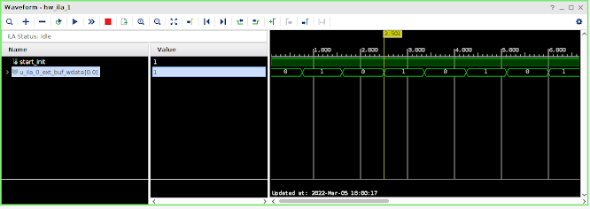
Read Levelling is eanbled by setting a bit in one of the registers in the DDR3 RAM. When this mode is enabled, any read command will yield a pattern of bits 01010101 on every DQ pin. So, on the Arty A7, where the RAM chip has a 16-bit databus, you will see the following data bursts, when doing a read in read levelling mode:

  • 0000
  • FFFF
  • 0000
  • FFFF
  • 0000
  • FFFF
  • 0000
  • FFFF
Indeed, putting the RAM chip in read levelling mode, is a quick way to check if we got our clock constraints correct with connectivity to the RAM.

One thing you might realise when capturing when capturing the test pattern, is that the alignment of the captured data is out by two or more bits. Let me explain why this can happen.

For any command we want to issue to the RAM chip, we need to supply 4 bits of data for every signal in the 83MHz clock domain, which will be clocked out by the OSERDESE2 in the 333MHz domain.

For a command, typically only 1 of these 4 bits will be the actual command. The rest of these bits will just be padded out either with ones or zeros.

For simplicity one might decide to pad out the first three bits and have the fourth bit as the command bit.

Now, as we all know, with the DDR family of chips, you don't get the requested data right away, but need to wait for a couple of clock cycles before you get the data.

For the RAM on the Arty A7 @333MHz, this waiting period is 5 clock cycles. This uneven number might cause that the burst of bits doesn't start on a 4 bit boundary.

To counter this, you would need to play with the position of the command bit within the four bits.

About the DQS signal during reads

During reads from DDR memory, we rely on the memory to provide us with a DQS signal, telling when we should strobe the data in the FPGA.

However, with my experimentation on the Arty A7, I found it basically impossible to constraint this signal coming from the outside, so that this signal can reliably clock an ISERDESE2.

Nevertheless, all hope is not gone. In the beginning of this post I mentioned that we can simplify a RAM controller on the Arty quite dramatically, because there is not really a need for doing levelling upon startup.

The read DQS signal is no exception to this. I found that we can use the same signal that is used for DQS write signal, to strobe the ISERDESE2 blocks for the data as well.

So, all in all I managed to capture data supplied by the RAM during read Levelling.

In Summary

In this post I talked a bit about read levelling. I also managed to enable read levelling mode on the Arty A7, and to read the data pattern provided by this mode successfully.

In the next post I will try and see if I can write some random data value to RAM, and read the same value back.

Till next time!

Saturday 5 March 2022

Write Levelling on the Arty A7

Foreword

In the previous post we looked at the Memory controller provided by the Elphel project, which is used in their 10393 camera model. This memory controller works on the Zynq, but since the Zynq is from the same family than the FPGA of the Arty A7, we should be able to use the design also on the Arty A7.

Also, in the previous post, we looked a bit into the DDR3 protocol. One of the extra steps involved in DDR3 compared to previous versions of RAM is write levelling and Read levelling.

In this post we will see if we can get the memory controller of the Elphel project to build for the Arty A7 and if we can get write levelling to work.

Delaying a signal coming out of an FPGA

In the previous post that with the DDR3 protocol one can delay the DQS signal for each byte lane so that it matches the command signals.

Let me explain in a bit more detail why DDR3 needs the delay feature for the DQS signal.


In the above diagram, we have three RAM chips connected to the Memory Controller. The purple line is the Clk/ Command/ Address lines. As you can see the distance for these signals is greater to chips 2 and 3 than to chip 1. For the data/strobe signals the distances are more or less the same to each chip.

Let us now see how these components will be wired up in a DDR2 setup:

You can see here the Data/Strobe signals (blue lines) looks more less the same as in the DDR3 scenario.

The Clk/Command/Address signal routing (purple) looks a quite bit different than with DDR3. In DDR2 these signals branch off in different directions, maintaining somewhat the same distance to the different memory chips. The drawback of this branching off is that you will end with some impedance issues at higher clock speeds.

DDR3 tries to address these impedance issues of the control signals by making use of daisy chaining, as shown in the DDR3 image earlier on. The drawback of daisy chaining, as I explained earlier, is that the control signals arrive at different times at the different memory chips. For this reason we need to delay the DQS signal for each memory chip by a certain amount, to compensate for the different arrival times of control signals at the various memory chips.

The amount of delay adjustment required is typically much less than the time of complete clock cycle. In general such delays can be implemented in an FPGA by having a couple of Flip-Flops in series and clocking these Flip-Flops at x times the required frequency. So, for instance if the required frequency is 5Mhz, and you want to delay this signal by one tenth, you can add one delay flip-flop clocking at 50MHz.

Similarly, to delay the 5 MHz by two tenths, you can have two flip-flops in series also been clocked by a 50MHz signal. 

Such a kind of solution will not work for delaying DQS signals to a DDR3 memory chip, because these delay flip-flops will be clocked beyond the limits of an FPGA. Just to take the Arty A7 as an example, where the RAM is clocked at 300MHz. Just to delay this signal by a 10th, you will need to clock a delay flip-flop with 3GHz. Way beyond the capabilities of the Arty A7 😀

Luckily Xilinx provides a way out of this problem with the help of ODELAYE2 and IDELAYE2 blocks. These blocks can be programmed to give these tiny amounts of delay. ODELAYE2 can delay signals going out of the FPGA and IDELAYE2 can delay signals coming into the FPGA.

There is a caveat for using a ODELAYE2 block: It is only available on pins of the FPGA in a specific bank, called the HP (High Performance bank). Fortunately for the memory controller of the Elphel 10393, all pins that serves the external DDR3 RAM is in the HP bank.

Unfortunately for us, who will be using the Arty A7 board, will not be so lucky. All pins on the FPGA that serves the DDR3 RAM on the Arty A7, is in the HR (High Rang) bank. So, ODELAYE2 is an unreachable luxury for us.

Luckily there is some tricks we can do with the Mix Mode Clock Manager (MMCM) for setting fine delays, which I will cover in the next section.

MMCM for fine delay

I MMCM is basically a block that takes as input a clock signal and outputs one or more clock signals, each of which the frequency can be different from the input clock. The frequency of an output clock can be either multiplied to be higher than the input frequency, or divided to be lower that the input frequency.

Another nice feature of the MMCM is that you can match the phase of the output clock with the phase of the input clock, or you can offset the phase of the output clock in relation to the phase of the input clock with a given amount.

This phase difference can be either fixed or dynamic. With fixed you can only set the phase of the output clock during design time, but with dynamic you can change the phase of the output clock while your design is running on the FPGA.

To enable dynamic you need to set the parameter CLKOUTx_USE_FINE_PS to TRUE on the block instance, where x is the clock number. As you might have guest, I am going to use this dynamic feature for changing the delay of the DQS signal.

With dynamic you can shift the phase of the output clock up or down one step at a time. One step is a 1/56th of the VCO clock period.

To shift the phase one step, you need to make use of the following signals:

  • PSCLK
  • PSEN
  • PSINCDEC
  • PSDONE
You signal whether you want to step up or down via the PSINCDEC input. To initiate the phase shift you need to ensure PSEN is asserted for one clock cycle of PSCLK.

Once the command is given, you need to wait for PSDONE to be asserted before giving another clock shift command.

With the memory controller we use from the Elphel project, there is an existing mmcm instance of which we can use one output for varying the delay for DQS. This mmcm instance is located in the following file: memctrl/phy/phy_top.v.

There is a number of changes that needs to be made to this module. In order to try and keep the discussion to the point, I am not going to go into details about this.

Trying out write levelling

To a DDR3 RAM chip from powerup to write levelling mode, involves quite a number of steps and setting a bunch of registers on the memory chip.

The designers of the Elphel 10393 decided to do all these steps in software, which simplifies the overall design.

In our case, doing DDR3 initialisation in software is not really an option for the Arty A7. If we were to perform the initialisation process via software, the program will need to be stored in block RAM, because DDR3 RAM is not available at powerup. Because Block RAM is such a precious resource on the FPGA, I have decided to perform the initialisation rather with a state machine.

In my experimentation with write levelling I am shifting the phase of the DQS signal non-stop, so I am expecting bit 0 of DQ to toggle now and again.

Inspecting a ILA waveform confirmed my theory:


This confirms that we are more or less on track. 

In Summary

In this post we played a bit with write levelling.

I was looking for something that could delay the DQS signal by small amounts. ODELAYE2 can do it, but is not an option on the Arty A7 because all DDR3 signals are connected to pins of an HR bank of the FPGA.

In the end I discovered that we can also achieve this delay via dynamic phase shifting provided by a MMCM.

Observations confirmed that write levelling can work by making use of an MMCM.

In the next post I will continue to experiment with write levelling and read levelling.

Till next time!