Tuesday 22 February 2022

Diving into an Opensource Memory Controller

Foreword

In the previous post I gave a quick run down of initials perceptions of the Arty A7 board in getting memory access to work.

The Memory Interface Generator (MIG) provided by Vivado is very easy to use to create blocks for interfacing with the memory on the Arty board. However, no matter how much I tweaked the MIG generated code, I couldn't get to a design with minimal latency.

I started looking into alternative opensource Memory Controller designs, with the hope of getting around this latency issue.

One of the opensource designs I have looked into in the previous post, was a ddr3 design by Ultraembedded on Github. This is a very simplistic design, but also have latency issues.

In this post I will look into another Opensource memory controller, which is provided on Github by the Elphel camera project.

The Elphel Camera project is quite a project of note, of which the DDR3 memory controller forms just one component of it. So, in order to understand the surrounding context of their memory controller, I will start at a very high level, explaining what the Elphel camera project is about, and then gradually zoom into the memory controller itself.

About Elphel Inc.

Elphel Inc. is a company that produces opensource digital cameras. It uses lenses and Image sensors from other manufacturers. These cameras processes the images from the image sensors and produces JPGs using an FPGA and a CPU. 

One of the notable customers for Elphel cameras was Google Street View. I am sure many people have seen a vehicle like this in their neighbourhood the past decade or so, which was used to capture the footage for Google Street View:


The spherical ball on top contains a couple of cameras pointing in different directions. Many of these balls contained Elphel cameras in the past. The interesting thing is that the hosted FPGA/CPU within the Elphel setup can handle a couple of image sensors simultaneously, where each sensor can be 5MP or higher. These cameras can capture a number of frames a second, convert it to JPG's and store it to a SATA hard drive. 

Through the years Elphel produced different camera models, with their most recent models using a SoC that contains both a CPU and an FPGA: The Xilinx Zynq 7030 SoC. This is the big brother of the Zynq 7010, which is used in the Zybo board.

Let us have a quick look at the block diagram for the 10393:


You will note that both the FPGA and the ARM core has its own RAM. As you have seen in my C64 series on the Zybo, you have seen that it is possible for the FPGA to also access the RAM used by the ARM CPU. However, in the case of the 10393 the memory access patterns is quite unique, and for that reason they have decided to give the FPGA access to its own RAM.

On Elphel's web site there is a very interesting blog post in all the thoughts that went into designing the FPGA memory controller:

https://www.elphel.com/www3/node/355

The nice thing here is that the FPGA embedded in the Zynq 7030, and the FPGA on the Arty A7 is from the same FPGA family, so it should be easy to use the 10393 memory controller on our Arty A7 board. However, as you will see later there is some minor tweaks we need to do to make it work on the Arty.

Focusing on the 10393 memory controller

Let us now focus on the 10393 memory controller. First of all, here is the link to the source code for the 10393:

https://github.com/Elphel/x393

The following diagram they provide gives a quick overview on how the components fit together:


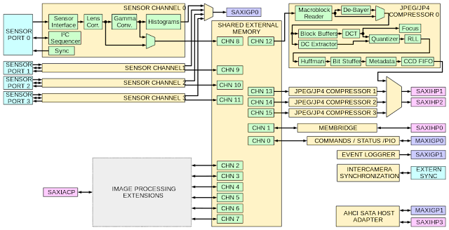
Shared External Memory is basically the memory controller, providing various channels for peripherals that need access to memory. The image sensors use channels 8, 9, 10 and 11 for writing image data to memory.

The blocks creating JPEGs for every sensor, uses channel 12, 13, 14 and 15 for reading from memory. Something interesting about these blocks is that they write the resulting JPEGs to the ports SAXIHP1 and SAXIHP2. These ports will ensure that this information ends up in the RAM to which the ARM CPU has access to, so that the JPEGs can be written to an SATA hard drive.

Looking at the code, it is quite difficult to figure out at first glance how the memory controller works. However, I have found it helps if you initially only focus on these files:

  • memctrl/mcntrl393.v
  • memctrl/memctrl16.v
  • memctrl/phy/mcontr_sequencer.v
  • memctrl/phy/phy_cmd.v
  • memctrl/phy/phy_top.v
Here mcntrl393.v is the top level module of the memory controller and the rest of the list is order by module level, so phy_top.v is the lowest level module.

Even with narrowing down to a handful of files, there is still a lot going onπŸ˜€. So, I will try and not be pedantic and just focus on what is required.

More on the DDR3 protocol

Before we get to see how we are going get the 10393 memory controller working on a Arty A7, let us familiarise ourselves a bit with the DDR3 protocol. This background information will help when we need to troubleshoot later on.

On a DDR3 RAM chip, you have the following signals:
  • Address
  • Cas - Column select
  • Ras - Row select
  • We - write enable
  • DQ - data
  • DQS - data strobe
  • Command clock
There is other signals on DDR3 chips as well, but for simplicity of this discussion, I am only showing these.

For anyone that is familiar with the RAM of a Retro gaming system, like the C64, many of the above signals will look familiar. For instance, on the C64 we know that in order to read from memory we first need to provide a row address, with the Ras signal asserted, and then  we need to provide a column address with the Cas line asserted. After some time, while the CAS line is asserted, the data will be available on the data lines.

As you can see from my description above, there is not really an exact times defined for when each of these steps should be performed. Luckily the manufactures of these RAM did provide for quite some headroom for timing errors.

However, throughout the years manufacturers tried pushing the data rate of RAM chips higher and higher, causing the headroom for timings errors to shrank drastically. To get around this increasing tight fit, it was necessary to introduce some clocking for both the commands and the data. For this reason there is a command clock and a DQS (Data Strobe) signal.

Another limitation when increasing the data rate is impedance and trace length, especially when you have multiple memory modules. The memory modules the furthest away from the memory controller will receive the controller signals (e.g. Cas, Ras, We, Command clock) later than the closer ones, causing clock skew.

In DDR3 we have the capability to compensate for these clock skew by delaying the DQS signal for each byte lane, so that it matches the Command Clock. The process of determining the amount of compensation required is called Write levelling and read levelling.

Let us have a quick look at how Write levelling work. We will look at read levelling in a later post.

With write levelling the DDR3 memory chip needs to placed first in write levelling mode. This is done by setting a register within the DDR3 memory chip.

During this mode the memory controller needs to toggle the DQS signal. However, during this mode the DDR3 memory chip uses the DQS signal in a totally different way than in normal mode of operation. In this mode, during the rising edge of the DQS signal, the memory chip samples the command clock and out the result on the lowest bit of the DQ bus. The purpose is that a '1' is eventually outputted on the DQ bus. If this is not the case, the DQS signal needs to be increasingly delayed in small steps, until a '1' is output to the DQ bus.

In Summary

In this post we have started to look into the memory controller provided by the Elphel Camera project especially from their 10393 camera model.

We also looked very briefly into the DDR3 protocol.

In the next post we will start to try and get this memory controller to work on the Arty A7 board.

As a first step, we will try and get write levelling to work, adjusting the DQS signal until we get a '1' on the DQ bus.

Till next time!

Saturday 12 February 2022

Initial steps with the Arty A7

Foreword

Hi All! It has been quite a while since my last post.

In my last post I was the bearer of bad news regarding getting an Amiga core to run on a Zybo FPGA, because the effective latency of the DDR RAM was just too much.

In the previous post I also hinted that the direction I want to take to solve this latency issue, was to use an FPGA board that can give us raw access to DDR RAM. The board I have earmarked for this exercise is the Arty A7.

In this post I will give some feedback on my initial findings on using the Arty A7 board.

Initial Impressions

Having previously worked with the Zybo quite a bit, I got quite accustomed to the building blocks the Zynq SoC provides you out the box. On the Zynq there are two ARM cores, which you can write software to perform the non-time-critical functionality, easing your brain a bit on thinking how to implement it in the FPGA. Also, accessing RAM in the FPGA of the Zynq is also fairly straightforward.

Lastly, the Zynq also provides a number of onboard peripherals, like USB, I2C which you also program in software, once again simplifying your FPGA design.

When turning to the Arty A7, it feels initially like you are handed a blank canvas. You handed a bunch of logic elements, but no ARM cores, no DDR RAM controller and no on chip peripherals. Here I must give some credit to Vivado, that does provide you some wizards that can generate some of the building blocks that the Zynq provide. However, these generated blocks do eat into your available elements in the FPGA. 

Let us have a quick look at some of the wizards provided in Vivado. One of the wizards will create a MicroBlaze CPU core for you. This is a CPU core created by Xilinx which you are free to use within Vivado.

Another Wizard that Vivado provides is the MIG (Memory Interface Generator) Wizard. As the name suggests, this provides you an interface for communicating with DDR RAM. One of the useful interfaces that MIG provides is an AXI interface. AXI is also the interface that is used between Peripherals and the FPGA in the Zynq chip.

The MicroBlaze processor also supports the AXI interface, so in effect it is easy for the MicroBlaze processor to access DDR RAM via the generated MIG memory interface.

As you might have gathered, I will be putting all my efforts into understanding the design the MIG will generate πŸ˜€ , obviously trying to limit memory latency as much as possible, so that it is usable in an Amiga design.

My experience with a MIG design

I have found that using the MIG wizard is relatively painless, and your FPGA design can have access to the onboard DDR3 RAM in no time.

However, with the MIG generated design I was faced once again with too much memory latency. I was convinced that AXI might be adding some extra latency, so I trying to see if the MIG does provide an alternative interface.

Indeed, I found in the MIG documentation that that the MIG does provide a native interface. Just by its name 'native interface', I was optimistic that I am up for minimal memory latency. Too my dismay, I found that the native MIG interface yielded no latency improvement πŸ˜•

It was time to bring the butcher knife and trying to butcher the generated MIG Verilog code, trying to find and ripping out any pipelining code that can potentially add to the latency.

Trying to customise the code generated by the MIG is also a story for another day. In Vivado, most of the generated code is read-only, so the only real way to edit it is to take all the generated source files and add it to a new project that is not MIG aware. In this process you also need to remember to move over all the necessary constraints.

After some pain, I got to a point where I could customise a generated MIG design. This allowed me to hunt down in the design where the latency is happening. The bad news was that the component causing the latency was a close source component, very tightly knitted in the MIG design. So, unfortunately it was not a case of throwing this component out and replacing with a different component.

So, in short it didn't seem possible to tweak a MIG design up to a point where you have minimised latency.

However, the whole exercise with  MIG wasn't a waste. One of the useful outputs from the MIG process is all the necessary constraints, like the pins of the FPGA that is connected to the DDR RAM chip.

Investigating alternative designs

With the bit of a dead end I have reached with the MIG, I started looking around for Memory Controller designs on the Internet, that is open source. In this process I did found a couple of possible candidates which I will discuss in the next post.

Out of interest, I will share a solution that looked very simple and promising on Github:

https://github.com/ultraembedded/core_ddr3_controller

The nice thing about this core is that it also designed to run on the Arty A7. The downside of this core is again its latency, which gave it a maximum throughput of 5MHz.

In Summary

In this post I gave my initial findings on the Arty A7 board.

I also gave a broad outline of the detours I took to attempt to get to a memory controller design with minimal latency. Unfortunately, I wasn't able in this post to get a solution.

In the next post we will look into another open source memory controller available on Github, that have some merit for what we want to achieve.

In the next post, I will also be covering details about the DDR3 protocol.

Till next time!