Foreword
In the previous post we looked at the Memory controller provided by the Elphel project, which is used in their 10393 camera model. This memory controller works on the Zynq, but since the Zynq is from the same family than the FPGA of the Arty A7, we should be able to use the design also on the Arty A7.
Also, in the previous post, we looked a bit into the DDR3 protocol. One of the extra steps involved in DDR3 compared to previous versions of RAM is write levelling and Read levelling.
In this post we will see if we can get the memory controller of the Elphel project to build for the Arty A7 and if we can get write levelling to work.
Delaying a signal coming out of an FPGA
In the previous post that with the DDR3 protocol one can delay the DQS signal for each byte lane so that it matches the command signals.
Let me explain in a bit more detail why DDR3 needs the delay feature for the DQS signal.

In the above diagram, we have three RAM chips connected to the Memory Controller. The purple line is the Clk/ Command/ Address lines. As you can see the distance for these signals is greater to chips 2 and 3 than to chip 1. For the data/strobe signals the distances are more or less the same to each chip.
Let us now see how these components will be wired up in a DDR2 setup:

The amount of delay adjustment required is typically much less than the time of complete clock cycle. In general such delays can be implemented in an FPGA by having a couple of Flip-Flops in series and clocking these Flip-Flops at x times the required frequency. So, for instance if the required frequency is 5Mhz, and you want to delay this signal by one tenth, you can add one delay flip-flop clocking at 50MHz.
Similarly, to delay the 5 MHz by two tenths, you can have two flip-flops in series also been clocked by a 50MHz signal.
Such a kind of solution will not work for delaying DQS signals to a DDR3 memory chip, because these delay flip-flops will be clocked beyond the limits of an FPGA. Just to take the Arty A7 as an example, where the RAM is clocked at 300MHz. Just to delay this signal by a 10th, you will need to clock a delay flip-flop with 3GHz. Way beyond the capabilities of the Arty A7 😀
Luckily Xilinx provides a way out of this problem with the help of ODELAYE2 and IDELAYE2 blocks. These blocks can be programmed to give these tiny amounts of delay. ODELAYE2 can delay signals going out of the FPGA and IDELAYE2 can delay signals coming into the FPGA.
There is a caveat for using a ODELAYE2 block: It is only available on pins of the FPGA in a specific bank, called the HP (High Performance bank). Fortunately for the memory controller of the Elphel 10393, all pins that serves the external DDR3 RAM is in the HP bank.
Unfortunately for us, who will be using the Arty A7 board, will not be so lucky. All pins on the FPGA that serves the DDR3 RAM on the Arty A7, is in the HR (High Rang) bank. So, ODELAYE2 is an unreachable luxury for us.
Luckily there is some tricks we can do with the Mix Mode Clock Manager (MMCM) for setting fine delays, which I will cover in the next section.
MMCM for fine delay
I MMCM is basically a block that takes as input a clock signal and outputs one or more clock signals, each of which the frequency can be different from the input clock. The frequency of an output clock can be either multiplied to be higher than the input frequency, or divided to be lower that the input frequency.
Another nice feature of the MMCM is that you can match the phase of the output clock with the phase of the input clock, or you can offset the phase of the output clock in relation to the phase of the input clock with a given amount.
This phase difference can be either fixed or dynamic. With fixed you can only set the phase of the output clock during design time, but with dynamic you can change the phase of the output clock while your design is running on the FPGA.
To enable dynamic you need to set the parameter CLKOUTx_USE_FINE_PS to TRUE on the block instance, where x is the clock number. As you might have guest, I am going to use this dynamic feature for changing the delay of the DQS signal.
With dynamic you can shift the phase of the output clock up or down one step at a time. One step is a 1/56th of the VCO clock period.
To shift the phase one step, you need to make use of the following signals:
- PSCLK
- PSEN
- PSINCDEC
- PSDONE
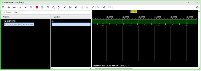
Trying out write levelling
No comments:
Post a Comment