In the previous post we managed to catch the scan codes of keys pressed on a USB keyboard.
In this post we will be redirecting these keystrokes to our C64 module so we can have some meaningful interaction with our C64 module.
The Plan of Action
Let us start by refreshing our minds a bit.
A couple of posts ago we implemented two slave registers which we mapped into memory space at locations 43c0_0000 and 43c0_0004.
Combining these two slave registers we have 64 bits in which each of these bits represents a key on the C64 keyboards. The ARM can toggle the bits in these registers and in effect simulate key presses within our C64 module.
All it will take from us is to take the USB keyboard scan codes we receive from the keyboard, and converting it to C64 key scan codes and we have a working implementation.
Starting simple
Let us start by implementing a mapping between USB and C64 keyboard for just four keys: A, B, C, D.
The USB scan codes for these keys are as follows:
A -> 4
B -> 5
C -> 6
D -> 7
The corresponding scan codes for these keys on a C64 is as follows:
A -> 0xa
B -> 0x1c
C -> 0x14
D -> 0x12
We can create a quick mapping function for these keys:
u32 mapUsbToC64(int usbCode) {
 if (usbCode == 0x4) {
  return 0xa;
 } else if (usbCode == 0x5) {
  return 0x1c;
 } else if (usbCode == 0x6) {
  return 0x14;
 } else if (usbCode == 0x7) {
  return 0x12;
 }
}
We will invoke this method within our state_machine method where are printing the USB scancodes to the console:
So, if the scancode is less than 32 we set the appropriate bit at address 0x43c0_0000. For scancodes bigger than 32 we set the appropriate bit at address 0x43c0_0004.
Implementing simultaneous key presses
Up to this point in time we are only able to deal with one key press at a time. This becomes an issue when we want to type double quotes (") on the C64, which require pressing the shift and the 2 key simultaneously.
In this section we will deal with simultaneous key presses.
Luckily from the USB side we are provided with enough information to determine if more than one key is pressed simultaneously. Each byte from the 8 bytes returned in the USB report descriptor represent a key that is currently been pressed. The exception to the rule is modifier keys, like Shift and Control. The status of all the modifier keys is contained within a single byte, where is bit corresponds to a modifier key.
We start off by creating a method we are sending the 8 USB bytes and returning the values we need to assign to addresses 0x43c0_0000 and 0x43c0_0004 respectively:
We implement two loops for looping through both USB words:
void getC64Words(u32 usbWord0, u32 usbWord1, u32 *c64Word0, u32 *c64Word1) {
  *c64Word0 = 0;
  *c64Word1 = 0;

  usbWord0 = usbWord0 >> 16;

  for (int i = 0; i < 2; i++) {
   int current = usbWord0 & 0xff;
   if (current != 0) {
     int scanCode = mapUsbToC64(current);
        if (scanCode < 32) {
     *c64Word0 = *c64Word0 | (1 << scanCode);
     } else {
     *c64Word1 = *c64Word1 | (1 << (scanCode - 32));
     }

   }

   usbWord0 = usbWord0 >> 8;
  }

  for (int i = 0; i < 4; i++) {
   int current = usbWord1 & 0xff;
   if (current != 0) {
     int scanCode = mapUsbToC64(current);
        if (scanCode < 32) {
     *c64Word0 = *c64Word0 | (1 << scanCode);
     } else {
     *c64Word1 = *c64Word1 | (1 << (scanCode - 32));
     }

   }

   usbWord1 = usbWord1 >> 8;
  }

}
You will see that for the first USB word we are discarding the first two bytes. This is because the first byte is the byte mask for the modifier keys and the second byte is reserved.
Talking about the modifier keys. It would be nice to implement the shift key in order to type the double quotation (") in our C64 module. So let us do that quickly:
In the previous post we managed to read a couple of descriptors from a USB keyboard and identified which endpoint to use for capturing the keystrokes from the keyboard.
In this post we will develop some code for actually retrieving the keystrokes from the keyboard.
Moving to the configured state
For the majority of the previous post we lingered within the default state. Just to refresh our minds again of the other states for a USB device, have a look a gain at a USB state diagram.
As you can see, after the Default state there is still two states, Address and Configured, we need to go through until we can do something useful with the USB device.
Let us start by having a look at the Address state. In this state we assign an address to our USB device so so that it stops listening at the default address (e.g. 0).
To set the address, we need to make a bit of changes to our state_machine method:
void state_machine() {
 //bit 24 bit 18
 u32 in2 = Xil_In32(0xE0002144) | (1<<24) | (1<<18);
 Xil_Out32(0xE0002144, in2); //clear

 if (status == 0) {
  set_port_reset_state(1);
  scheduleTimer(12000);
  status = 1;
  return;
 } else if (status == 1) {
  set_port_reset_state(0);
  status = 2;

  //set address
  Xil_Out32(0x301000, 0x00030500);
  Xil_Out32(0x301004, 0x00000000);
  schedTransfer(1,0,0x0, 0x300000);
  return;
 } else if (status == 2) {
  scheduleTimer(3000);
  status = 3;

  return;

 }
}
Here we are setting up a request type 5, which is SET_ADDRESS, and we are setting the device to address 3. We end by waiting 3 milliseconds just make sure everything settled down before we continue.
Let us now configure the device. For his we implement an extra status in our if-else block:
You will see that we adjust the device address in our first address to 3, because the address was changed in a previous state.
Next we select the appropriate configuration. In the previous post we determined that we should select configuration number #1.
At this stage our USB device is fully configured and ready to use.
A brief pause at periodic schedules
With our USB keyboard ready to use, the next thing obviously for us is to read the keystrokes.
My first take on reading these keystrokes was to also implement an asynchronous schedule. However, with this approach I didn't had any luck at all. Things worked better for me using Periodic schedules.
So, in this section let us spend some time discussing in more detail how periodic schedules work.
Firstly, let us look again at the diagram of how periodic schedules work. Have a look again at the diagram on page 446 of the Zynq TRM.
From the diagram we see that everything is driven of a periodic frame list been referenced in part by a
FrameIndex, which is updated at the end of each USB frame.
A USB Frame is basically a time period of 1 millisecond.
If you look into further detail on when the FrameIndex gets updated, you will see that strictly speaking the frameindex isn't updated every millisecond, but every 1/8 millisecond. Furthermore you will see that the bottom 3 bits of the FrameIndex is not used to index the Periodic frame list, but rather from bit 3 upwards of the frameindex.
At this point you my be wondering why the frameindex get incremented every 1/8 of a millsecond if the rest of the system only work in increments of 1 millisecond.
The answer is to maintain a bit of compatibility between USB 1.1 and USB 2.0. USB 1.1 always had frames of 1 millisecond in duration. USB 2.0 introduced the concept of microframes, breaking a framedown into even smaller durations of 1/8 milliseconds.
But, despite my explanation, how can you access 1/8 millisecond frames if the frame index, for all basic reasons, only gets incremented every 1 milliseconds? The key to this questions lies in the lower 8 bits of word 2 in a QH.
From the EHCI spec these 8 bits is referred to as the Interrupt schedule mask. Every bit in this byte correspond to a specific microframe within the frame. A one in any particular position means that the transaction will take place within the particular microframe.
If only one bit is set within the Interrupts schedule mask, only one transaction will execute within the frame. Similarly, if more than one bit is set, more than one transaction will trigger within the frame.
Let us now talk a bit about the data structures a Period Frame List points to. A Periodic Frame List also points to QH/qtd structures as an Asynchronous List does.
In fact, it is very convenient to think of each element in a Periodic Frame List as an Asynchronous list on its own. In this analogy, each element of the Periodic Frame List can be thought of as an ASYNCLISTADDR-register on its own.
There is , however, a small flaw in this analogy. In an Asynchronous schedule the ASYNCLISTADDR-register gets updated during traversal to always point to the next QH in the list. In a periodic schedule, however, each element in the Periodic Frame List always point to the first QH element in the list.
As such, within a periodic schedule a circular QH list doesn't make sense.
Configuring the Periodic Schedule
Let us now write some code for scheduling the periodic schedule.
Firstly we need to specify the number of elements of our Periodic Frame List. We want to poll once every 16 milliseconds. Since each element have duration of 1 millisecond, it makes sense to have sixteen elements with only one of these elements pointing to a valid QH.
To set the frame list size we make use of three bits of register 0xe0002140: 15, 3 & 2. These three bits gets grouped together as [15][3][2] and has the following meaning:
000: List size is 1024 elements
001: List size is 512 elements
010: List size is 256 elements
011: List size is 128 elements
100: List size is 64 elements
101: List size is 32 elements
110: List size is 16 elements
111: List size is 8 elements
From the above list we should use the value 110 which corresponds to the following code:
You might find it a bit strange that we start with a QH that doesn't contain any qTD's at all, followed by a QH that does have them. I will explain the reasoning behind this a bit later on.
You will also see that the NAK count reload field for the second QH is zero. You might recall that for our asynchronous Schedule this was always 15. Why the difference?
To answer this question let us first look at what a NAK packet is.
When a USB host request data from a USB device and the device doesn't have any data available it will respond with a NAK packet. Sometimes you would like to throw an error if a certain number of NAK packets is received in a row. This is the purpose of the NAK reload field.
In our case we just would like to ignore these packets all together, so we set the RL field to zero. In our schedule when a NAK packet is encountered the slot will just be ignored and be moved on to the next slot.
What is left to be done is to enable the periodic schedule by adding another state within state_machine:
As can be seen, we schedule a wait of 10 milliseconds before we transition the next state.
Reading the actual keystrokes
Let us now write some code for capturing keystrokes from the USB keyboard.
The basic idea is to display the keycode each time a key is pressed or released.
In the previous post we have set up the periodic scheduled with a scheduled qTD transfer in one slot.
We should poll this qTD datastructure till the transfer is finished, which happens when bit 7 of word 2 change to 0. We implement this functionality with an extra state:
We are polling the qTD datastructure at every 10 milliseconds. Once transfer is finished we will get the keystroke information at the first eight bytes at location 0x305000.
Once the scheduled transfer is finished, a new transfer would not be automatically scheduled. It is up to you to schedule a new one.
One could probably just reset the values in the qTD to restart a new transfer. Doing this we may end off with a potential cache coherency issue.
Changes you made to QH and qTD structures are written to System Memory. The DMA block within the USB controller reads these reads these changes from Main Memory from time to time into internal Dual-Port RAM.
One cannot tell at which stage the USB Controller is reading from System memory and half baked qTD datastructures might end up into the Dual port RAM.
The solution to this issue is to not modify these structures but to create new structures:
As you see, this is where our QH comes in which contains no qTD's. Once we have created a new QH and qTD we just change the next pointer of the first mentioned QH.
One thing to also keep in mind when a transfer is complete, is to preserve the Data toggle bit and apply it to the new qTD. This is done as follows:
All the developed code should now be sufficient to capturing the keystrokes continuously and outputting to the console.
The meaning of USB keycodes
As mentioned in the previous section, each key press will result in 8 bytes been populated at address 0x305000. However only the last 6 bytes is significant to us.
Each value of these six bytes represent a keycode of a key that is currently pressed. This means that up to 6 keys can be pressed simultaneously.
USB key scan codes is a bit different than your convential PS/2 codes in that it is more predictable. For instance have a look at the USB scan codes for the first couple of alphabet letters:
Key A: scancode 4
Key B: scancode 5
Key C: scancode 6
Key D: scancode 7
Key D: scan code 8
Key E: scancode 9
etc.
In summary
In this post we implemented some code for catching keystrokes from the USB keyboard.
In the next post we will integrate the USB keyboard with our C64 module.
In the previous post we discussed a bit of theory surrounding USB communications and started to implement some interrupts from the USB functional block in the Zynq.
In this post we will get a bit more practical and see how to reset a USB device and to read configuration information from it.
In this post we will not be implementing functionality to detect when a device is plugged or unplugged, in order to keep things simple. We will thus assume a USB keyboard is attached on the USB port when we start up.
The Life Cycle of a USB Device
To get a bit of context of for this post, let us look at the life cycle of a USB device. There is a couple of states involved.
The attached state is the state when you have just attached a USB device into the USB port.
Provided the USB host enabled a voltage between the VCC pin and GND pin on the USB port, the USB port will power up and enter the Powered state shortly after attachment.
It should be noted, though, that when a USB Host was just powered up, no voltage will be present on the VCC+GND pins. It is up to you to configure the USB Hub so that power is enabled over these two pins.
Once a USB is in the powered state, it still will not respond to any Host commands over the ports. You first need to apply a reset over the USB port so that the device enter the Default state.
When a USB device is in the default state, it will respond to traffic on device address 0 and on endpoint 0.
It should be noted that the USB device will not stay in the default state for long, probably for a couple of tens of milliseconds, at most. It is up to you to get the device to the address state as soon as possible.
At the addressed state the USB will be assigned a non zero-address and all subsequent communication will be directly to this new address.
For the USB device to become fully functional it needs to transition to the configured state.
For the purpose of this post, we will just be moving to the default state and requesting a device descriptor and requesting a configuration descriptor. More on these descriptors later on.
Switching Port power on and resetting device
Let us get to writing some code.
First thing we should do, is to switch the USB module to Host mode. For this we need to use the lower three bits of register 0xe00021a8. The function of these three bits is defined as follows:
Next, we should switch on the port power. Bit 12 of register 0xE0002184 performs this task for us. So let us extend our method initUsb:
void initUsb() {
 Xil_Out32(0xE00021A8, 3);//set to host mode
 u32 in2 = Xil_In32(0xE0002184) | 4096;
 Xil_Out32(0xE0002184, in2); //switch port power on
}
The code above will bring our USB device into the power state. Next we need to reset the device to bring it into the Default state. Bit 8 of register 0xe0002184 is used to initiate port reset. So, let us create the following method to assert reset and to de-assert the reset:
Now, if one read through the USB 2.0 specification, it looks like we need to allow at least 12ms for USB device to come out of reset. Here we will make use of the state_machine method we defined in the previous post to assist in scheduling the 12ms delay:
...
void state_machine() {
   u32 in2 = Xil_In32(0xE0002144) | (1<<24) | (1<<18);
   Xil_Out32(0xE0002144, in2); //clear

   if (status == 0) {
    set_port_reset_state(1);
    scheduleTimer(12000);
    status = 1;
    return;
   } else if (status == 1) {
    set_port_reset_state(0);
    status = 2;
   } else if (status == 2) {
    printf("\n");
   }


}
...
int main()
{
     Xil_DCacheDisable();
     init_platform();
     initint();
     initUsb();
     status = 0;
     state_machine();
     usleep(100000000);
     cleanup_platform();
     return 0;
}
A you might remember from the previous post, we are using the state_machine method as a callback when an interrupt happens within the USB block of the Zynq. Here, however we are also calling it from the main method. We do this just as the initial state for our state machine.
In this initial state we assert the port reset and schedule the timer for 12ms. After the 12ms an interrupts will trigger and the state_machine method will be called again. This time around we will de-assert the port reset. At this stage our USB keyboard should be in the default state listening for USB traffic on address 0.
It is in this default state we can read the device descriptor and the configuration descriptor from the USB device.
In order to read these descriptors from the device, we need to schedule an asynchronous schedule, which we briefly touched on in the previous post. To schedule this, we need to know more about the following datastructures: Q Head (QH) and q Transfer descriptors (qTD). We will discuss this in the next section
Q Heads and Transfer descriptors
Let us have a look at the QH and qTD data structures.
First the QH data structure. This structure is discussed within the Zynq TRM on page 463.
The first word in the structure is a pointer to the next QH. For our Asynchronous schedule, the first QH will just be pointing to itself.
The second word have a couple of fields of importance:
RL (NAK counter reload): For our case we will just use a value of 15
C (Control endpoint flag). Set this field to a one if it is a non High Speed, control endpoint. We will indeed set this field to one in our case.
Maximum Packet length: We will be setting this field to 8.
H (Head of reclamation list). Set this value to one, since we be having one, and one only QH
DTC (Data toggle control). Set to one
EPS (End Point Speed):
00: Full Speed
01: Low Speed (What we will be using)
10: High Speed
11: Reserved
EndPt (End point address): Since we will be using using the Control Endpoint, this value will be set to zero
I: Set to zero
Device Address: Since we will be operating when the device is in the default state, we will use device address zero
For the third word, I will not going into detail. We will just be using the value 0x40000000.
You will see that the remaining words is coloured in grey and according to the legend this means Host Controller Read/Write. We will leave all these zero, accept for Next qTD Pointer, in which we will specify the first qTD.
Let us now move unto the qTD structure. This structure is discussed on page 459 in the Zynq TRM.
The first word is a pointer to the next qTD structure.
The third word contains the following fields:
DT: Data toggle
Total Bytes: To Bytes to receive from or send to USB device
IOC: Cause an interrupt when this transfer is finished
C_Page (Current Page): Index to the current buffer (e.g. 0 to 4)
Cerr (Error counter)
PID (PID Code): More on this in the following section
00 Out
01 In
02 Setup
Status
Buffer Pointers 0 to 4: Four pointers, each of whicg points to a 4KB buffer. This contains the data received from or to send to the USB device that is assoaiated with this transfer descriptor.
Data Transfers from USB devices
One of the data-structures we covered in the previous section was transfer descriptors. A Transfer descriptor is what its name implies, that is to transfer data to or from the USB device.
According to the USB 2.0 specification, you get a couple of different types of Transfer, but in this post we will only focusing on one type: Control Transfers. The following web page does quite a good job of explaining control transfers, together with some diagrams:
This web page basically states that a Control Transfer can be broken down into a couple stages. To narrow down the number of scenarios, I am just going to focus on one particular use case: Getting a device descriptor from the USB device via the Control endpoint.
With this use case in mind, let us have a look at the different stages for a Control transfer.
Setup stage
The setup stage starts by issuing a setup token to the USB device. This indicates to the USB device what kind of data is about to follow.
Next follows a data packet. In our use case where want to request a device descriptor, this packet would contain this request to the USB device as such.
The USB would acknowledge the whole request with a ACK packet, indiacted by the white block in the diagram.
This whole stage would be taken care of by a transfer descriptor as discussed in the previous section. Interestingly, for this stage a PID would specified.
The data packet for this request would be contained in a buffer pointed to buffer pointer 0 contained in word 3 of the relevant qTD.
The Data Stage
In the data stage there are two scenarios. The first scenario is when we expect data back from the USB device and the second scenario is is we are required to send data to the USB device after the setup phase.
For our Use case we are only interested in the first scenario. For this we need need to setup a qTD with a PID of one. The Buffer pointer in this qTD will be a pointer to the buffer that will receive the data from the USB device during the Data Packet Phase.
Don't worry about the Handshake packet for now. This will be covered in the next phase.
The Status Stage
With our Use case we are receiving data from the USB Device, so it is up to us to acknowledge this data during the status stage.
For this stage we need to create a qTD with a PID of zero. Since we will be sending a data packet of zero length, we don't need to specify a valid buffer pointer in this qTD.
Initialising the Async queue
Now with a bit of theory behind, let us write some again. This time we will initialise the async queue.
Since our application is a bare-metal application, we will not be making use of malloc calls to allocate memory for our data structures. Instead, we will use some specific memory locations for our data-structures.
We start off by clearing the memory region we will be using for our data structures:
void initUsb() {
 Xil_Out32(0xE00021A8, 3);//set to host mode
 u32 in2 = Xil_In32(0xE0002184) | 4096;
 Xil_Out32(0xE0002184, in2); //switch port power on

 for (int i = 0; i < 1000000; i = i + 4) {
  u32 current = 0x300000 + i;
  u32 *currentword;
  hello = currentword;
  *currentword = 0;
 }
}
This will clear 1 Million bytes worth of words to zero starting at address 0x300000.
Next, we should setup a QH and a couple of qTD's. To assist us with this, we first need to create a helper data structure, making it easy to navigate through the 4 byte word nature of these data-structures:
void initUsb() {
...
 struct QStruct *qh;
 qh = 0x300000;
 qh->word0 = 0x300002;
 qh->word1 = 0xf808d000; //enable H bit -> head of reclamation
 qh->word2 = 0x40000000;
 qh->word3 = 0;
 qh->word4 = 0x300040;// pointer to halt qtd
 qh->word5 = 1;// no alternate

}
This QH starts at memory location 0x300000. The next pointer points back to itself (e.g. the first word).
You will also release that this pointer ends with 2 instead of zero. This is because bit 1 and 2 actually represents the head type of the pointer, which in this case is a QH.
Word 4 is a pointer to the first qTD of this QH, which starts at address 0x300040.
Word one has the value 1, menaing there is not a valid next qTD.
For word2 we specify a value of 0x40. This create us a async schedule in the halt state. We can now enable the async schedule:
void initUsb() {
...
 Xil_Out32(0xE0002158,0x300000); // set async base
 in2 = Xil_In32(0xE0002140) | 0x1;
 Xil_Out32(0xE0002140,in2); //enable rs bit
 in2 = Xil_In32(0xE0002140) | 0x20;
 Xil_Out32(0xE0002140,in2); // enable async processing

}
The async schedule is started by setting bit 5 of register 0xe0002140. Once enabled, the scheduler looks at register 0xe0002158 as the location for the first QH.
As mentioned, this async is now in the halt state. We need to add additional qTD's to make this schedule do something useful.
We will cover this in the next section.
Setting up a Transfer
Int he previous section we managed to enable an async, although not a very useful one: everything is in the halted state!
Let us start by creating a method for enabling a useful transfer:
void schedTransfer(int setup, int direction, int size, u32 qh_add) {

}
Setup specify whether we should add a setup qTD.
Direction specify whether we want to receive or send data. For receiving direction should be a 1.
Size is the number of bytes we want to send or receive.
qh_add is the address of the QH at which we want to add the qTD's.
If we require a setup token, we convert the halt qTD to a setup qTD:
You will see that the lower eight bits of word2 is still 0x40. This means that our queue will remain in the halt state till we change it another value.
This method advances to the next address and return to 0x300040 after a couple of advances, in effect simulating a circular buffer.
Reading a descriptor from USB Device
With the method created in the previous section, we can now use it to read a descriptor from the USB device.
To get the descriptor we need to schedule the transfer with the command request stored in a buffer. The USB 2.0 spec give us an indication on how this looks like on page 250:
Let us have a look at the values. We start with bmRequestType with value 0x80.
For bmRequest we need to use the constant GET_DESCRIPTOR. To get this value scroll down to the next page of the USB 2.0 spec and you will see the value is 6.
Descriptor Type is retrieved from the next table and have value 1 for Descriptor type DEVICE.
Wlength has value 0x12.
We can now modify our state_machine method to send a DEVICE_DESCRIPTOR request:
As seen, we are writing the request to the buffer at address 0x301000.
The descriptor returned by the USB device will be stored at location 0x302000. The else statement for status 2 can be used to print the contents of this buffer. Let us have a look at the contents of the buffer:
Since bytes are stored with an ARM core is little endian, for each word you should read the bytes from right to left.
So, we start off with 0x12 which is the length of the Descriptor.
0x1 is the Descriptor typem which in this case is DEVICE.
The next two bytes indicates the USB version which in this case is 1.1.
The next couple of bytes gives information of the Device class which is zero for three bytes. This means more info about the device is provided in the Configuration descriptor.
Following that is the maximum packet size which is 8 bytes.
Then there is a couple of vendor, product versions.
The last number of the descriptor is a 1 meaning that there is only one possible configuration.
That concludes our discussion on getting and reading the DEVICE descriptor.
Reading the Configuration Descriptor
Time for us to read the configuration descriptor. For this wee need to modify our state_machine method again:
00 -> string index for textual description. In this case none available
0xA0 -> couple of attributes
0x32 -> max power in 2mA units. In this case 100mA
From the configuration descriptor we see that two interfaces are defined. Each interface has the descriptor type number 4. Further more, byte 5 of this interface descriptor specify the interface type. For both these interfaces this is type 3, which is an HID(Human interface device).
The next two bytes of interest of the Interface descriptors is byte 6 and 7. For the first interface descriptor these bytes are 1 and 1, whereas for the second one it is 0 and 0.
For the first interface these two bytes corresponds to the following:
Boot interface Subclass
Keyboard
This type of Interface is a simplified keyboard interface for BIOS's and we will indeed use this Interface for our design.
Let us now go and have a look at the endpoint for this Interface.
07 05 81 03 08 00 0A
0x81 specify that this is an IN endpoint and the address of this endpoint is 1.
The 3 specifies that this in an interrupt endpoint.
The 8 specifies that the maximum packet size for this endpoint is 8 bytes.
The 0x0A specify the polling interval in milliseconds. Thus in this case the polling interval is 10 milliseconds.
In Summary
In this post we managed to read a couple of descriptors from a USB keyboard and isolated an endpoint that we can use to read keystrokes from the keyboard.
In the next post we will attempt to read keystrokes from the USB keyboard.
In the previous post we managed to implement the flashing cursor and keyboard interaction.
At this point in time a keypress can only be simulated by running a program on the ARM core that writes a value to a specific register and we are not yet at a point of integrating a physical keyboard to our C64 system.
The goal I have in mind is to integrate with a USB keyboard. To do this there is an easy way and a difficult way.
The easy way is way is to make use of PetaLinux, a Linux distribution provided by Xilinx for the Zynq processor. Going this route will give you some USB and keyboard drivers simplifying our integration with a USB keyboard, avoiding to worry about the technicalities of the USB protocol.
Then there is the difficult route, trying to access the USB keyboard in Standalone mode. In standalone mode you cannot make use of the drivers that comes bundled with Linux, and you sort of need to re-invent the wheel for USB keyboard interaction.
Re-inventing the wheel is not really cool, but it gave me some second thoughts. I have been using USB devices for almost 18 years without knowing how the communication work between the PC and a USB device.
Going the difficult route is actually an opportunity to learn how USB works and in the next couple of posts (two or three?) we are going to do just that.
We are going to start off with a bit of theory on USB protocols and will gradually work our way to a practical implementation.
I am not going to implement a full USB protocol stack, but just bear minimum that is necessary to catch keystrokes from a USB keyboard.
A note about the source code
I have received a couple of requests to publish the full source code for the project in its current state.
Within the Readme.md I am going some instructions on how to create the project files and building the project.
USB Protocol Overview
When you plug a USB keyboard into your PC your PC is known as the USB host and the keyboard as the USB device.
A USB can support one or more functions. Let us have a quick look at an example where a USB device can support more than one function.
Say, for example, a manufacturer brings out a USB-webcam. The manufacturer might also decide to also ship the device drivers on the web cam itself and surface it to your PC as a Mass Storage Device.
Cool solution, but how will your PC differentiate between these two functionalities on the same set of USB wires?
The answer is to give each functionality an endpoint number. When your PC communicates with the USB device, it always need to provide an endpoint number so that the USB device knows for which function the message is intended for.
Let us now move onto the topic on how USB devices are addressed. USB devices are connected to the PC in a star topology.
Star topology is the same topology used on a Commodore 64 to attach multiple drives and printers to the single serial port on the C64.
A quirk with the star topology is that all devices can see all traffic of each other. To avoid confusion a unique address needs to be assigned to each device.
On C64 disk drives you make use of jumpers on each drive to assign the address.
On USB devices you don't have jumpers. So, how are the addresses assigned?
The answer is that you just need to reset a device, then it will be in the default address state and respond on requests on Address zero.
At this point the alert reader will say: 'Aha! You just said USB uses a start topology, so won't reset signal reset all the USB devices?'
Yes it is, but a USB reset signal is one of the signals a USB host has finer control of, and you can limit a reset to a specific to a specific USB port.
Let us conclude our Overview of USB by having a look at how communication is orchestrated between the devices and the Host.
USB communication among the devices and the host is orchestrated by means of Host polling.
This means that the host initiates all communication. Even if a USB device have some information that urgently needs the attention of the host it needs to wait for the host to ask it for the information.
EHCI
Back to the ZYBO board. If you have a look in the ZYNQ 7000 manual, you will see that it provide some information on how to establish communication between your Zybo board and a USB device.
However, when working on your USB implementation, you will probably find that the information provided within this Technical Reference manual is simply not enough to give you a clear direction on where to go.
Doing an Internet search on how to implement USB on the Zybo board will probably also not be fruitful either.
I almost went into despair over this, till I found that the USB specific registers on the Zynq is not specific to the Zynq only, but follows a specific standard known as ECHI (Enhanced Host Controller Interface).
The thought that the USB implementation was not Zynq specific, actually widened my horizon and immediately was able to find more implementation examples. In fact, I could find a nice example within the Linux source tree.
To communicate with USB devices, the EHCI standard defines two schedules into which you can queue USB communication requests: Periodic schedule & Asynchronous schedule.
You make use of the Periodic schedule if you want to poll specific USB devices for information at specific time intervals. This will typically be for USB devices like USB sound cards giving a stream of information at a fixed data rate. On page 446 of the Zynq technical reference, it is explained how the periodic schedule is implemented.
We will cover in more detail how this schedule is setup at a later stage.
There might be cases where you don't want to poll a USB device constantly for information, but in a more adhoc fashion as the need arises. For this you will make use of asynchronous queues. On page 448 of the Zynq reference manual, it is explained how asynchronous queues works.
The interesting part in the diagram is where it mentions Insert and Remove QH's as needed, just reiterating its adhoc nature. When you are at a point of not needing any information from the Async Queue at the moment, you will just have a Queue Head pointing to itself been in one or other Halt state.
When you suddenly need some information again from a particular USB device, you can add a Queue head to the Queue, which will be processed and the Queue will return back to a halt state.
We will cover setup of the Asynchronous queue also at a later stage.
Writing some code
We have covered quite of theory. Let us now see if we can start writing some code.
Programming a USB interface have quite some detail, and one can a bit overwhelmed so that you don't know where to start. But, we can always start with small steps.
Let us start with the following:
Getting Caching right
Enabling Interrupts
Starting with getting the Caching right. In order to set up a periodic queue or an async queue, you need to write some data structures directly to SDRAM. When an ARM core writes these structures, the data-structures might not end up in SDRAM straight away, but will linger for some time in an L1 or an L2 datacache.
There are a couple of ways to deal with this potential caching issue. I am just going to take a simple approach and disable the Data Cache all together:
I have added so long most of the common headers we will need over time for our USB exercise. The headers together with the associated libraries is provided by the Xilinx SDK when you compile your program as a standalone.
Let us us now move onto interrupts. The USB module present within the Zynq provides interrupts for two timer expiry events, and USB events like when transfers is completed. These are very useful interrupts indeed which we would like to intercept.
It is therefore necessary to enable the above mentioned interrupts and ensure one of our custom methods gets called when they happen.
To configure interrupts on the Zynq (and probably most ARM based SoC's) is quite a mission.
So, in effect you need to figure how to program the Generic Interrupt controller and then how to enable interrupts on the ARM processor.
Luckily the Xilinx SDK provided some wrappers for shielding most of the complexity for us.
A strip down version for enabling the interrupts will looks as follows:
...
int help;
int myhelp;
XScuGic_Config *IntcConfig;
XScuGic INTCInst;
...
void state_machine();
...
void initint() {

 IntcConfig = XScuGic_LookupConfig(0);
 int status;
 myhelp = 1;

 status = XScuGic_CfgInitialize(&INTCInst, IntcConfig, IntcConfig->CpuBaseAddress);
 Xil_ExceptionRegisterHandler(XIL_EXCEPTION_ID_INT,
         (Xil_ExceptionHandler)XScuGic_InterruptHandler,
      &INTCInst);
 Xil_ExceptionEnable();
 status = XScuGic_Connect(&INTCInst,
         53,
         (Xil_ExceptionHandler)state_machine,
         (void *)myhelp);
 XScuGic_Enable(&INTCInst, 53);

}
...
void state_machine() {
}
...
int main()
{
    Xil_DCacheDisable();
    init_platform();
    initint();
    cleanup_platform();
    return 0;
}
Within the method initint we basically configure the GIC and enable interrupts on the ARM processor.
Also, in the code we are enabling Shared Peripheral Interrupt (SPI) #53. All USB block related interrupts will trigger via this interrupt.
We also configure so that our custom method state_machine will be called each time a SPI interrupt #53 happens. We will fill the method state_machine during the course of time.
You might realise that the method call XScuGic_Connect accepts a fourth parameter, which in this case we just passed a pointer to an integer called myhelp.
Usually for this parameter you will pass a pointer to a driver structure and when an interrupt happens, your interrupt handler (which in this case is state_machine) will receive this pointer as a parameter.
In our case we will not be using this parameter in our interrupt handler. Instead, we be implement a state machine within our interrupt handler and define a global status variable that will keep track of the current state.
One final thing needs to be done with our interrupt initialisation and this is to enable the applicable USB interrupts.
We would like to enable the General Purpose Timer Interrupt 0 (GP0). We also would like to enable Async Interrupts so that an interrupt is triggered when an Asynchronous transfer has completed.
During our journey to create a USB interface one of the things we will often do is to schedule a timer to wait a certain amount of time before performing the next task.
One can certainly use the sleep or usleep function provided by the SDK wrappers, but I am not so sure how accurate those are.
For the purpose of scheding timers, I am going to make use of General purpose timer 0 provided by the USB block.
This timer works in a very similar fashion as timers you find on a CIA 6526. You load a timer value into a load register, and then force this value to load into a running a timer register. The timer will count down from the predetermined value until it reaches zero and cause an interrupt.
On the Zynq, the timer load value register is located at 0xe0002080. This counter clocks at 1MHz (exactly the same as the CIA on C64). This register is 24 bits wide and can thereforebe set to up to 16 seconds.
To read the current value of the timer you need to read memory location 0xe0002084. The current timer value is present in the lower 24 bits. Bit 31 and bit 30 of this register is also of impotance for us:
Bit 31: Timer enable
Bit 30: Timer reset. When setting this bit to a one the timer will be reloaded with the value stored in location 0xe0002080
With this information, it is clear that we should setup the timer using the following steps:
Load the required timer value into 0xe0002080
Reload the timer by writing 1 to bit 30 of 0xe0002084
Start the timer by writing a 1 to bit 31 of 0xe0002084
I added the usleep in the main method so that our program isn't exited prematurely.
After 3 seconds the message Timer finished will be displayed on the console.
The write to location 0xe0002144 at the beginning of the state machine needs to done to ensure that the interrupt that just happened is cleared. Without this state_machine will be executed in an endless loop.
In Summary
In this post we covered some theory regarding USB.
We also started to write some for disabling data caching and enabling the appropriate USB interrupts.
In the next post we will implement functionality for resetting a USB device and configuration info from it in its default state.
Welcome back! It has been a while since I played around with my C64 FPGA implementation, so I first had to familiarise myself with where I was and where do I want to go 😊
In the previous post I managed to show the C64 Welcome message on the VGA screen, but without any flashing cursor.
In this post we will be implementing the flashing cursor, as well as implementing keyboard interaction.
Implementing the flashing cursor
To implement the C64 flashing cursor on our FPGA implementation, we should just ensure we interrupt our 6502 at a regular interval of 60 times per second.
To do this, we first need to implement a counter for this:
Here we have created a counter counting down from 16666 to zero and then reloading it with a value of 16666. Since we are clocking it with the 1 MHz signal, the counter will underflow at a rate of 60Hz, which is what we need.
We will use this clock to generate our interrupt signal:
    always @(posedge clk_1_mhz)
    if (c64_reset)
      int_occ <= 0;
    else if (counter_60_hz == 0)
      int_occ <= 1;
    else if (addr == 16'hdc0d & we == 0)
      int_occ <= 0;
As you can see we are setting int_occ to a one when our counter reaches zero. At this stage we should mimic CIA 6526 behaviour, meaning that once an interrupt happens the interrupt status for this interrupt should remain set until cleared by software.
The interrupt status gets cleared by simply reading the interrupt status register and this is done with the else statement else if (addr == 16'hdc0d & we == 0).
Great, we can now generate an interrupt 60 times per second and all we need to do is hooking up this signal to our 6502 core:
Let us now continue to implement keyboard interaction.
Keyboard Interaction
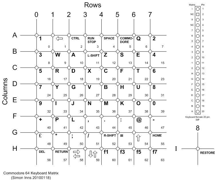
Within a real C64 the keys of its keyboard is arranged electrically as an 8x8 square matrix.
This 8x8 matrix in turn is hooked up to Port A and Port B of CIA#1.
Port A energises specific rows in the 8x8 matrix and Port B can see which keys within the energised row is either open or closed.
The following diagram gives an idea of how the keys is arranged within the matrix:
On the top right you can get an idea of how the keyboard connector looks like.
I am not in possession of a real C64, so we will need to make use of a USB keyboard and take the keystrokes and emulate C64 keystrokes.
So, how do we go about with this keyboard emulation? Well, firstly if you have a look at the diagram above, you will see all the keys is numbered from 0 to 63.
This gives us 64 possible keys, each one that can be either on or off. Each key can therefore be thought of as a bit.
Thinking of the memory space of our two ARM cores living on the ZYNQ, each memory location is 32 bits wide. Thus, we could fit all the possible C64 keys within two memory locations!
Is is then up to us to write a program running on the ARM processor, fetching keystrokes from the USB keyboard, and toggling the desired bits within above mentioned two memory locations to emulate the desired C64 key presses.
The previous paragraph sounds like a mouthful, so let us try to break it down a little. We need to achieve the following:
Interface with the USB keyboard and interpret keystrokes
Enable our C64 module to receive data from one of the ARM cores, also located on the ZYNQ
Emulate the C64 keypress with the data we received from one of the ARM cores.
To interface with the USB keyboard can be quite challenging task. At this point in time I don't want to elaborate too much, but towards the end of this post I will reveal a plan of action to get to a point of getting input from a USB keyboard 😀
Looking at the second point. In order for our C64 module to receive information from a ARM core, we need to engage the road of AXI Slave interfaces. We will cover this a bit a later in this post.
We will the third point, C64 keypresses emulation in the next section.
C64 Keypress emulation
Let us now continue to implement the C64 key press emulation.
We start off by adding two ports to our C64 module:
We should now think how should emulate the keyboard behaviour. Remember, port A on CIA#1 energise the applicable row, and we read the result via port B.
So, for starters we should capture 6502 writes to port A, which is address $DC00:
I might be worthwhile to mention that we are working here with active when high logic, because it makes live easier. You might recall though that the C64 works with active low logic.
So to work between these two worlds, we negate the value received from port A, and when you send the calculated value back to port B we negate it again.
Connecting to the outside World
With the changes perfoemd to our C64 module, we need a way to interface to an ARM core. This is where we need to work again with AXI's.
In previous posts we worked a couple of times with AXI's. The AXI's we worked with previously were all AXI Masters.
We defined an AXI Master for writing frames produced by our VIC-II to SDRAM. We also defined an AXI Master for reading back these frames from SDRAM by our VGA module and generating a VGA signal for displaying these frames on screen.
An AXI Master can be seen as a source for generating memory requests.
In our case where we need to receive data from an ARM core, we need something the opposite, which is receiving memory orders. An AXI peripheral receiving memory orders, is called an AXI Slave.
You can create an AXI block which contain both an AXI slave and an AXI master. The following is an example:
This is within our existing design.
Marked in green is the new AXI slave port called S00_AXI and in red is our existing AXI Master port called M00_AXI.
You will also see that I have also hooked the two slave port as indicated also in green. To enable these two ports on the AXI block, I had to some custom code changes which I will cover now.
With our AXI open in IP Packager, scroll to the user port section and change it as follows:
One of the things you will realise when you configure an AXI module to have an AXI slave interface, is that an AXI slave module will automatically be created and an instance be created within the top module. The instance within the top module will look something like the following:
These registers basically forms the heart of the AXI slave interface. In effect it is these registers that will map at a specific address in address space, and if one of the ARM cores to a write to this address range, the contents of the write will end off in one of these slave registers.
It is the content of these registers which we want to propogate to our C64 module to inform it which key was pressed. More on this later.
The following snippet is also interesting:
 always @( posedge S_AXI_ACLK )
 begin
   if ( S_AXI_ARESETN == 1'b0 )
     begin
       slv_reg0 <= 0;
       slv_reg1 <= 0;
       slv_reg2 <= 0;
       slv_reg3 <= 0;
     end
   else begin
     if (slv_reg_wren)
       begin
         case ( axi_awaddr[ADDR_LSB+OPT_MEM_ADDR_BITS:ADDR_LSB] )
           2'h0:
             for ( byte_index = 0; byte_index <= (C_S_AXI_DATA_WIDTH/8)-1; byte_index = byte_index+1 )
               if ( S_AXI_WSTRB[byte_index] == 1 ) begin
                 // Respective byte enables are asserted as per write strobes
                 // Slave register 0
                 slv_reg0[(byte_index*8) +: 8] <= S_AXI_WDATA[(byte_index*8) +: 8];
               end
           2'h1:
             for ( byte_index = 0; byte_index <= (C_S_AXI_DATA_WIDTH/8)-1; byte_index = byte_index+1 )
               if ( S_AXI_WSTRB[byte_index] == 1 ) begin
                 // Respective byte enables are asserted as per write strobes
                 // Slave register 1
                 slv_reg1[(byte_index*8) +: 8] <= S_AXI_WDATA[(byte_index*8) +: 8];
               end
           2'h2:
             for ( byte_index = 0; byte_index <= (C_S_AXI_DATA_WIDTH/8)-1; byte_index = byte_index+1 )
               if ( S_AXI_WSTRB[byte_index] == 1 ) begin
                 // Respective byte enables are asserted as per write strobes
                 // Slave register 2
                 slv_reg2[(byte_index*8) +: 8] <= S_AXI_WDATA[(byte_index*8) +: 8];
               end
           2'h3:
             for ( byte_index = 0; byte_index <= (C_S_AXI_DATA_WIDTH/8)-1; byte_index = byte_index+1 )
               if ( S_AXI_WSTRB[byte_index] == 1 ) begin
                 // Respective byte enables are asserted as per write strobes
                 // Slave register 3
                 slv_reg3[(byte_index*8) +: 8] <= S_AXI_WDATA[(byte_index*8) +: 8];
               end
           default : begin
                       slv_reg0 <= slv_reg0;
                       slv_reg1 <= slv_reg1;
                       slv_reg2 <= slv_reg2;
                       slv_reg3 <= slv_reg3;
                     end
         endcase
       end
   end
 end
This code starts off by saying that at a reset, all slave registers is been initialised to a zero.
During a write operation the applicable slave register gets written in the case statement.
What remains to be done is to surface the contents of the first two slave registers as two output ports in this module:
...
 // Users to add ports here
        output wire [31:0] slave_reg_0,
        output wire [31:0] slave_reg_1,
 // User ports ends
...
 // Add user logic here
    assign slave_reg_0 = slv_reg0;
    assign slave_reg_1 = slv_reg1;

 // User logic ends
...
These ports should then be connected all the way to the top module, which we can then connect to our C64 module.
With the ports added and everything hooked up, you will see in the address editor a section in address space is reserved for this slave interface:
With this address map, when have a program running on the ARM core and it writes to either address 0x43c0_0000 or 0x43c0_0004, the content will arrive at our C64 module at the two slave ports.
The Test Program
With our block design completed, we need to write a small C program that will run on one of the ARM cores to test the design.
This test program should basically set one of the bits in the two slave registers to trigger a simulated keypress.
For the program, the following main method will do:
...
int main()
{
    init_platform();
    Xil_Out32(0x43c00000,0x100);
    return 0;
}
...
This program sets bit 8 of the slave register. Bit 8 in this register corresponds to scancode 8, and should therefore type a '3' on the C64 screen.
A Test Run
Time to do a quick Test Run. The following video shows the result:
The video starts off with a flashing cursor and shortly afterwards a '3' gets printed when the program executes.
It works!
In Summary
In this post we managed to implement the flashing cursor as well as implementing key press simulation.
Well, obviously to make our live easier it would be nice to capture keystrokes from a real keyboard, which in our case would be an USB keyboard.
This is where things can really get interesting.
Firstly, we can make our life easy by installing PetaLinux on our Zybo board. This is a version of Linux and have drivers that will take care of all USB communications and detecting keyboard strokes for us.
When running the Zybo board in Standalone mode, you cannot make use of these USB/keyboard drivers and you will need to develop something yourself.
This is where my Hacker instinct starts to kick in and the eagerness to learn how stuff works that we all takes for granted.
This is an excellent opportunity to learn how USB works, so I thought of dedicating a couple of posts on developing a stripped down USB protocol stack.
So, in the next post I will spend some time on a bit of theory on how USB communications work and then take it from there.
In the previous post we managed to display a static frame stored in SDRAM to a VGA screen.
In this post we are going to take it one step forward and try to display frames rendered from our VIC-II module to a VGA screen.
To View a Video for this Post...
This video explains how to modify our current C64 design to take output the frames from our VIC-II module and display it on a VGA screen.
For a more in detail discussion on the contents of this video, please continue reading...
A recap on the current state of our C64 design
It has been some time since we worked on our C64 design.
In the last couple of posts all efforts was diverted into developing functionality for displaying frames stored in SDRAM to a VGA screen.
Within goal accomplished in the previous post, I think it is time we focus again on our C64 design.
So, let us start by refreshing our minds where we ended off with our C64 design.
When we last worked on the C64 design, it was in a state where we could generate a VIC-II frame with the C64 welcome screen, and store it in SDRAM.
So, with the functionality from the previous post where we could display a frame from SDRAM to a VGA screen, we should be able see the C64 welcome screen displayed on a VGA screen.
One things to mention though is that our design from the previous post expects frames to be at the exact resolution of the VGA monitor you are using. Our C64 design, however, produces frames at a much lower resolution (e.g. something like 404x284).
We will therefore need to modify our VGA block to cater for the resolution produced by our C64 design.
Modifying the VGA output block
As mentioned in the previous section, our C64 block produces frames that is lower in resolution than a typical recent VGA monitor.
On the over hand, since most recent VGA monitors are LCD's, it is best to produce VGA signals having the native resolutions of the VGA screen in question. It just looks better on these screens in native resolutions.
In this post we will therefore output a signal at native resolution and display the C64 output frames in small section on the screen.
This requirement requires a couple of changes to our VGA block design.
The first change is within our Asynchronous FIFO that buffer that buffers pixel data from the AXI clock domain to the pixel clock domain:
With this change we only enable reads from this FIFO when our VGA signal is at the visible region on the screen.
The visible region is between vertical position 100 and 384 and between horizontal position 100 and 505. This will give as the small 404x284 C64 window on the screen.
We would like our small C64 window to be surrounded by a black border on the screen. To that we need to do the following modifications:
With this change we output the pixel data from our FIFO if it is within the visible region. For all other positions we output a black pixel.
Adding VGA output to our C64 design
Let us now add VGA output to our C64 design. We do this by first adding the VGA block mentioned in the previous section.
Next, we add the AXI Read block we have developed and used in the last couple of posts.
We will wire up this VGA and AXI read block in a similar way as described previously. Care should however be taken with the AXI Master output port of our AXI read block.
When adding the VGA functionality to our existing C64 design, we will have indeed have two AXI master ports we will need to hookup, whereas our current Processing system only have one AXI slave port configure.
We will therefor need to twig our design a bit to cater for the two master ports.
Start off by removing all AXI helper blocks. I have highlighted them in the following picture:
With these blocks removed, we need to configure our Processing block by double clicking on it, and selecting an extra GP port:
With this option selected, you will see an extra AXI GP port on the processing block:
You can now make use of the designer assistance provided by the IDE to wire up both GP ports.
Just after the wiring up, you will most probably get the following warning:
The IDE will nonetheless allow you to continue, but you will eventually be stopped with an actual error during either the Synthesis or Bitstream generation process. So it is better to try and resolve the warning at this point.
Let us see if we can resolved this warning. We start by opening the Address editor tab within Block design window:
The values in the address editor is used to configure the AXI Helper blocks to decide to which GP port to forward a particular address. But, there is a bit of duplicate mappings here. For instance, the 512MB block range starting at address 0x0 is mapped to both GP0 and GP1.
We can simplify the mapping the following:
Now we have GP0 dedicated to our AXI write block and GP1 dedicated to our AXI read block.
With these changes our design should Synthesise and generate the BitStream without any errors.
The End result
With everything started up, the screen looks as expected:
This is only the Welcome screen with no Flashing cursor.
In Summary
In this post we managed to display the frames produced from our VIC-II module to the VGA screen.
In the next post we will attempt to implement the flashing cursor.
In the previous post we attempted to view random data in SDRAM as a static frame on the VGA screen.
We, however, ended with a random alternating pattern displayed instead of a random static pattern.
In this post we will attempt to fix this anomaly.
To view a Video of this Blog...
This video explains with the help of a Xilinx community post that the cause of the non static frame displayed was likely caused by the asynchronous FIFO implementation used. I also show how I apply the suggestions from the Community post to my existing post in order to fix the problem...
If you rather prefer the written version together with a discussion on the actual changes to the Verilog code, please continue reading...
Some help from a old community post
The anomaly encountered in the previous post really baffled me, and I didn't know where to actually start looking for the cause of the problem. So, I consulted the Internet...
In my searching I came across the following post on a Xilinx Community forum:
The member was experiencing some serious timing violations when trying to synthesise the design.
The key to the solution was provided by the community member with the nickname Avrumw. He pointed out that in the comments of the mentioned design it was suggested that the design follows some recommendations from a Xilinx article. Avrumw, however had some serious doubts whether Xilinx would make some of these suggestions at all because of the following (I am quoting from Awrumw's answer):
- It uses a latch
- It uses the asynchronous preset/clear inputs of flip-flops for part of its functionality
The suggestions Awrum gave to avoid these practices was the following:
- infer the RAM
- use Gray counts for bringing addresses between domains
- use standard "two back to back flip-flop" synchronizers (with the ASYNC_REG property set) to move the Gray coded read pointer into the write domain (for generating full) and the Gray coded write pointer into the read domain (for generating empty)
Admittedly, the design on Asic World did indeed made use of Gray Counters.
Let us know proceed and see if we can apply these suggestions to our design
Applying the suggestions to our design
From the suggestions, the first thing I am going to do, is make use of back-back flip synchronizers.
We will need a set of two of these back-back synchronizers. One for passing pNextWordToWrite to the read side and another one for passing pNextWordToRead to the write side.
The ASYNC_REG annotation will ensure that the flip-flops for each synchroniser set will be placed closed to each other when synthesising the design.
These flip-flops will be assigned as follows:
//write synchroniser
//--------------------------------------------------------------------------------------
     always @(posedge WClk)
     begin
       synchro_write_side_0 <= pNextWordToRead;
       synchro_write_side_1 <= synchro_write_side_0;
     end
//---------------------------------------------------------------------------------------

//read synchroniser
//--------------------------------------------------------------------------------------
     always @(posedge RClk)
     begin
       synchro_read_side_0 <= pNextWordToWrite;
       synchro_read_side_1 <= synchro_read_side_0;
     end
//---------------------------------------------------------------------------------------
Please take note that each synchroniser gets clocked by a different clock.
Let us now see where these synchronisers will get used. Before we continue, I would just like to mention that I had to deuplicate the code for tboth the write side and the read side. So, let us first start with the code on the write side:
Here we have replaced all instances of pNextWordToRead with synchro_write_side_1.
Next, let us get rid of the transparent latch. First, let us have a look at the original code that inferred a transparent latch:
    //'Status' latch logic:
    always @ (Set_Status, Rst_Status, Clear_in) //D Latch w/ Asynchronous Clear & Preset.
        if (Rst_Status | Clear_in)
            Status = 0;  //Going 'Empty'.
        else if (Set_Status)
            Status = 1;  //Going 'Full'.
If you look closely at the code, you will identify many scenarios where there will be no assignment. In those scenarios we need to revert to one or other previous stored state. For this reason the above code will be inferred as a transparent latch.
To eliminate the need for a transparent latch we need to split the above into pieces that will infer into a pure computational logic block and a storage element. The result is as follows:
So, we have a pure storage element Status_write_prev_side that store the contents of the computational block Status_write_side at each clock cycle. So, in the case where there is no assignment happening for Status_write_side, we can just output the value of Status_write_prev_side.
Next, let us see what we can do to eliminate the need for a flip flop with an asynchronous preset. First, let us look again at the original code that will infer a flip-flop with an asynchronous preset:
    //'Full_out' logic for the writing port:
    assign PresetFull = Status & EqualAddresses;  //'Full' Fifo.

    always @ (posedge WClk, posedge PresetFull) //D Flip-Flop w/ Asynchronous Preset.
        if (PresetFull)
            Full_out <= 1;
        else
            Full_out <= 0;
Looking at this piece of code, one can immediately see why they needed to use an asynchronous flip-flop. In deriving PresetFull we had to use some values that gets assigned in the read clock domain. So, it would make sense to trigger the assignment the moment PresetFull transitions from a zero to a one rather than waiting for the Wclk to transition. In this way we can avoid a setup and hold violation.
However, with Xilinx FPGA's we still try and avoid these asynchronous presets. Since we safely moved over pNextWordToRead from the read domain to the write domain, we don't need such manoeuvres. So, the assignment of Full_out, just simplifies to:
I can confirm that the mentioned changes did in fact solve my issue and a static random pattern was displayed on screen.
I wanted to show a picture in this post on how the screen looks like with these changes, but the photo is not very clear. I better exercise would be to display a meaningful photo on the VGA screen.
To do this exercise we will make use of the XSCT console to write the contents of a image file to the SDRAM of the ZYBO board.
Needless to say, this image file will need to contain raw pixel data in the format RGB565. The file format that comes close this is Microsoft's BMP format. Interesting enough, GIMP allows us to create a BMP file in the RGB565 format.
To do this open up the image you want to convert in GIMP and then select File/Export As.
Give a filename, suffix it with a .bmp extension and hit export. Specify the options in the option window as follows and hit the export button again:
We will then use this file and write its contents to the SDRAM of the Zybo board. You should remember though that the image file doesn't start with raw image straight away, but rather from byte offset 0x46 as deduced via the following article on Wikipedia:
So, because our image frame starts at address 0x200000 in Zybo SDRAM we should write our file at the address starting at 0x200000 - 0x46 to account for the header. Thus, we should write our file to SDRAM starting at address 0x1fffba.
With our Zybo board programmed and a program been kicked off via the Xilinx SDK, we should issue the following command via the XSCT console:
mwr -size b -bin -file /home/johan/Downloads/bm1360.bmp 0x1fffba 3000000
Obviously you need to specify your own file name.
With the image data written our VGA display looks as follows:
Static image indeed.
In Summary
In this post we fixed the issue where a non static image was shown onscreen.
This issue was caused by the following unsafe practices :
Using transparent latches
Using flip-flops with asynchronous presets.
In the next post we will attempt to display the output from our VIC-II to the VGA screen.