Foreword
Welcome back! It has been a while since I played around with my C64 FPGA implementation, so I first had to familiarise myself with where I was and where do I want to go 😊In the previous post I managed to show the C64 Welcome message on the VGA screen, but without any flashing cursor.
In this post we will be implementing the flashing cursor, as well as implementing keyboard interaction.
Implementing the flashing cursor
To implement the C64 flashing cursor on our FPGA implementation, we should just ensure we interrupt our 6502 at a regular interval of 60 times per second.To do this, we first need to implement a counter for this:
    always @(posedge clk_1_mhz)
    if (c64_reset | counter_60_hz == 0)
      counter_60_hz <= 16666;
    else
      counter_60_hz <= counter_60_hz - 1;
Here we have created a counter counting down from 16666 to zero and then reloading it with a value of 16666. Since we are clocking it with the 1 MHz signal, the counter will underflow at a rate of 60Hz, which is what we need.
We will use this clock to generate our interrupt signal:
    always @(posedge clk_1_mhz)
    if (c64_reset)
      int_occ <= 0;
    else if (counter_60_hz == 0)
      int_occ <= 1;
    else if (addr == 16'hdc0d & we == 0)
      int_occ <= 0;
As you can see we are setting int_occ to a one when our counter reaches zero. At this stage we should mimic CIA 6526 behaviour, meaning that once an interrupt happens the interrupt status for this interrupt should remain set until cleared by software.
The interrupt status gets cleared by simply reading the interrupt status register and this is done with the else statement else if (addr == 16'hdc0d & we == 0).
Great, we can now generate an interrupt 60 times per second and all we need to do is hooking up this signal to our 6502 core:
    cpu mycpu ( clk_1_mhz, c64_reset, addr,
                          combined_d_out, ram_in, we, int_occ, 1'b0, 1'b1 );
That is all there is to get the cursor flashing.
Let us now continue to implement keyboard interaction.
Keyboard Interaction
Within a real C64 the keys of its keyboard is arranged electrically as an 8x8 square matrix.This 8x8 matrix in turn is hooked up to Port A and Port B of CIA#1.
Port A energises specific rows in the 8x8 matrix and Port B can see which keys within the energised row is either open or closed.
The following diagram gives an idea of how the keys is arranged within the matrix:
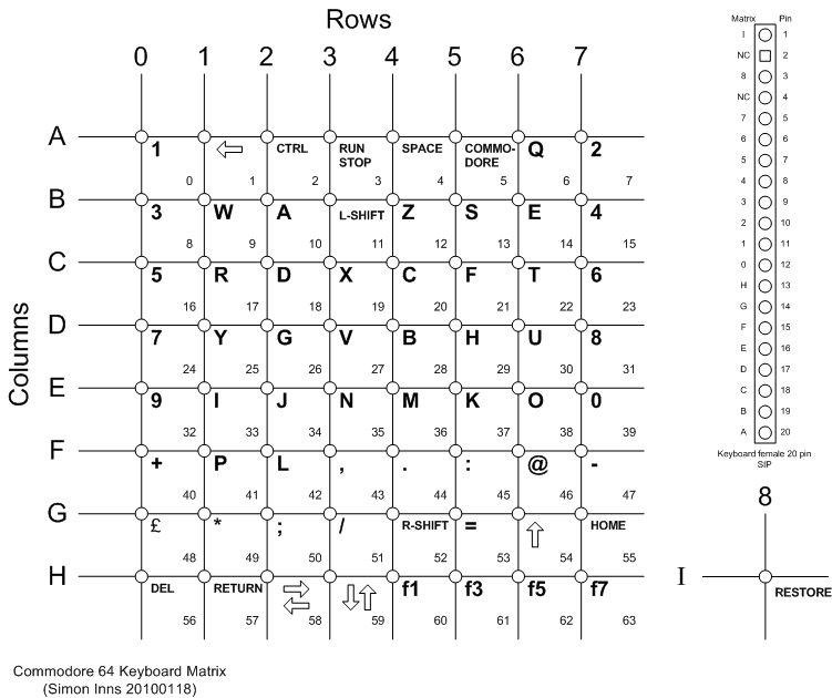
On the top right you can get an idea of how the keyboard connector looks like.
I am not in possession of a real C64, so we will need to make use of a USB keyboard and take the keystrokes and emulate C64 keystrokes.
So, how do we go about with this keyboard emulation? Well, firstly if you have a look at the diagram above, you will see all the keys is numbered from 0 to 63.
This gives us 64 possible keys, each one that can be either on or off. Each key can therefore be thought of as a bit.
Thinking of the memory space of our two ARM cores living on the ZYNQ, each memory location is 32 bits wide. Thus, we could fit all the possible C64 keys within two memory locations!
Is is then up to us to write a program running on the ARM processor, fetching keystrokes from the USB keyboard, and toggling the desired bits within above mentioned two memory locations to emulate the desired C64 key presses.
The previous paragraph sounds like a mouthful, so let us try to break it down a little. We need to achieve the following:
- Interface with the USB keyboard and interpret keystrokes
- Enable our C64 module to receive data from one of the ARM cores, also located on the ZYNQ
- Emulate the C64 keypress with the data we received from one of the ARM cores.
To interface with the USB keyboard can be quite challenging task. At this point in time I don't want to elaborate too much, but towards the end of this post I will reveal a plan of action to get to a point of getting input from a USB keyboard 😀
Looking at the second point. In order for our C64 module to receive information from a ARM core, we need to engage the road of AXI Slave interfaces. We will cover this a bit a later in this post.
We will the third point, C64 keypresses emulation in the next section.
C64 Keypress emulation
Let us now continue to implement the C64 key press emulation.
We start off by adding two ports to our C64 module:
module block_test(
  input clk,
  input axi_clk_in,
  input proc_rst,
  output proc_rst_neg,
  output wire [31:0] ip2bus_mst_addr,
  output wire [11:0] ip2bus_mst_length,
  output wire [31:0] ip2bus_mstwr_d,
  output wire [4:0] ip2bus_inputs,
  input wire [5:0] ip2bus_otputs,
  input wire [31:0] slave_0_reg,
  input wire [31:0] slave_1_reg
    );
These two ports are the two words as mentioned in the previous section, where each bit corresponds to a key on the C64 keyboard.
The following diagram gives an explanation of each bit. The number in each bit position is the relevant C64 scancode.

Next, we should split these 2 words into separate rows:
...
    wire [7:0] keyboard_row_0;
    wire [7:0] keyboard_row_1;
    wire [7:0] keyboard_row_2;
    wire [7:0] keyboard_row_3;
    wire [7:0] keyboard_row_4;
    wire [7:0] keyboard_row_5;
    wire [7:0] keyboard_row_6;
    wire [7:0] keyboard_row_7;
...
    assign keyboard_row_0 = slave_0_reg[7:0];
    assign keyboard_row_1 = slave_0_reg[15:8];
    assign keyboard_row_2 = slave_0_reg[23:16];
    assign keyboard_row_3 = slave_0_reg[31:24];
    assign keyboard_row_4 = slave_1_reg[7:0];
    assign keyboard_row_5 = slave_1_reg[15:8];
    assign keyboard_row_6 = slave_1_reg[23:16];
    assign keyboard_row_7 = slave_1_reg[31:24];
...
So, for starters we should capture 6502 writes to port A, which is address $DC00:
...
    reg [7:0] keyboard_control_byte;
...
    always @(posedge clk_1_mhz)
    if (addr == 16'hdc00 & we)
      keyboard_control_byte <= ram_in;
...
Next, we should simulate the value for Port B, which is address $DC01:
...
    wire [7:0] keyboard_result_byte;
...
    assign keyboard_result_byte = (~keyboard_control_byte[0] ? keyboard_row_0 : 0) |
                                  (~keyboard_control_byte[1] ? keyboard_row_1 : 0) |
                                  (~keyboard_control_byte[2] ? keyboard_row_2 : 0) |
                                  (~keyboard_control_byte[3] ? keyboard_row_3 : 0) |
                                  (~keyboard_control_byte[4] ? keyboard_row_4 : 0) |
                                  (~keyboard_control_byte[5] ? keyboard_row_5 : 0) |
                                  (~keyboard_control_byte[6] ? keyboard_row_6 : 0) |
                                  (~keyboard_control_byte[7] ? keyboard_row_7 : 0);
...
    always @*
        casex (addr_delayed)
          16'b101x_xxxx_xxxx_xxxx : combined_d_out = basic_out;
          16'b111x_xxxx_xxxx_xxxx : combined_d_out = kernel_out;
          16'hd012: combined_d_out = line_counter;
          16'hdc01: combined_d_out = ~keyboard_result_byte;
          default: combined_d_out = ram_out;
        endcase
...
I might be worthwhile to mention that we are working here with active when high logic, because it makes live easier. You might recall though that the C64 works with active low logic.
So to work between these two worlds, we negate the value received from port A, and when you send the calculated value back to port B we negate it again.
Connecting to the outside World
With the changes perfoemd to our C64 module, we need a way to interface to an ARM core. This is where we need to work again with AXI's.In previous posts we worked a couple of times with AXI's. The AXI's we worked with previously were all AXI Masters.
We defined an AXI Master for writing frames produced by our VIC-II to SDRAM. We also defined an AXI Master for reading back these frames from SDRAM by our VGA module and generating a VGA signal for displaying these frames on screen.
An AXI Master can be seen as a source for generating memory requests.
In our case where we need to receive data from an ARM core, we need something the opposite, which is receiving memory orders. An AXI peripheral receiving memory orders, is called an AXI Slave.
You can create an AXI block which contain both an AXI slave and an AXI master. The following is an example:

This is within our existing design.
Marked in green is the new AXI slave port called S00_AXI and in red is our existing AXI Master port called M00_AXI.
You will also see that I have also hooked the two slave port as indicated also in green. To enable these two ports on the AXI block, I had to some custom code changes which I will cover now.
With our AXI open in IP Packager, scroll to the user port section and change it as follows:
 // Users to add ports here
        input wire [31:0] ip2bus_mst_addr,
        input wire [11:0] ip2bus_mst_length,
        input wire [31:0] ip2bus_mstwr_d,
        input wire [4:0] ip2bus_inputs,
        output wire [5:0] ip2bus_otputs,
        output wire [31:0] slave_reg_0,
        output wire [31:0] slave_reg_1,
 // User ports ends
One of the things you will realise when you configure an AXI module to have an AXI slave interface, is that an AXI slave module will automatically be created and an instance be created within the top module. The instance within the top module will look something like the following:
 myip_burst_test_v1_0_S00_AXI # (
  .C_S_AXI_DATA_WIDTH(C_S00_AXI_DATA_WIDTH),
  .C_S_AXI_ADDR_WIDTH(C_S00_AXI_ADDR_WIDTH)
 ) myip_burst_test_v1_0_S00_AXI_inst (
  .S_AXI_ACLK(s00_axi_aclk),
  .S_AXI_ARESETN(s00_axi_aresetn),
  .S_AXI_AWADDR(s00_axi_awaddr),
  .S_AXI_AWPROT(s00_axi_awprot),
  .S_AXI_AWVALID(s00_axi_awvalid),
  .S_AXI_AWREADY(s00_axi_awready),
  .S_AXI_WDATA(s00_axi_wdata),
  .S_AXI_WSTRB(s00_axi_wstrb),
  .S_AXI_WVALID(s00_axi_wvalid),
  .S_AXI_WREADY(s00_axi_wready),
  .S_AXI_BRESP(s00_axi_bresp),
  .S_AXI_BVALID(s00_axi_bvalid),
  .S_AXI_BREADY(s00_axi_bready),
  .S_AXI_ARADDR(s00_axi_araddr),
  .S_AXI_ARPROT(s00_axi_arprot),
  .S_AXI_ARVALID(s00_axi_arvalid),
  .S_AXI_ARREADY(s00_axi_arready),
  .S_AXI_RDATA(s00_axi_rdata),
  .S_AXI_RRESP(s00_axi_rresp),
  .S_AXI_RVALID(s00_axi_rvalid),
  .S_AXI_RREADY(s00_axi_rready),
 );
Let us now have a look at the code for this module, looking only at the interesting parts of the code, though.
You will see that there is a couple of slave registers defined within this module:
...
 reg [C_S_AXI_DATA_WIDTH-1:0] slv_reg0;
 reg [C_S_AXI_DATA_WIDTH-1:0] slv_reg1;
 reg [C_S_AXI_DATA_WIDTH-1:0] slv_reg2;
 reg [C_S_AXI_DATA_WIDTH-1:0] slv_reg3;
...
These registers basically forms the heart of the AXI slave interface. In effect it is these registers that will map at a specific address in address space, and if one of the ARM cores to a write to this address range, the contents of the write will end off in one of these slave registers.
It is the content of these registers which we want to propogate to our C64 module to inform it which key was pressed. More on this later.
The following snippet is also interesting:
 always @( posedge S_AXI_ACLK )
 begin
   if ( S_AXI_ARESETN == 1'b0 )
     begin
       slv_reg0 <= 0;
       slv_reg1 <= 0;
       slv_reg2 <= 0;
       slv_reg3 <= 0;
     end
   else begin
     if (slv_reg_wren)
       begin
         case ( axi_awaddr[ADDR_LSB+OPT_MEM_ADDR_BITS:ADDR_LSB] )
           2'h0:
             for ( byte_index = 0; byte_index <= (C_S_AXI_DATA_WIDTH/8)-1; byte_index = byte_index+1 )
               if ( S_AXI_WSTRB[byte_index] == 1 ) begin
                 // Respective byte enables are asserted as per write strobes
                 // Slave register 0
                 slv_reg0[(byte_index*8) +: 8] <= S_AXI_WDATA[(byte_index*8) +: 8];
               end
           2'h1:
             for ( byte_index = 0; byte_index <= (C_S_AXI_DATA_WIDTH/8)-1; byte_index = byte_index+1 )
               if ( S_AXI_WSTRB[byte_index] == 1 ) begin
                 // Respective byte enables are asserted as per write strobes
                 // Slave register 1
                 slv_reg1[(byte_index*8) +: 8] <= S_AXI_WDATA[(byte_index*8) +: 8];
               end
           2'h2:
             for ( byte_index = 0; byte_index <= (C_S_AXI_DATA_WIDTH/8)-1; byte_index = byte_index+1 )
               if ( S_AXI_WSTRB[byte_index] == 1 ) begin
                 // Respective byte enables are asserted as per write strobes
                 // Slave register 2
                 slv_reg2[(byte_index*8) +: 8] <= S_AXI_WDATA[(byte_index*8) +: 8];
               end
           2'h3:
             for ( byte_index = 0; byte_index <= (C_S_AXI_DATA_WIDTH/8)-1; byte_index = byte_index+1 )
               if ( S_AXI_WSTRB[byte_index] == 1 ) begin
                 // Respective byte enables are asserted as per write strobes
                 // Slave register 3
                 slv_reg3[(byte_index*8) +: 8] <= S_AXI_WDATA[(byte_index*8) +: 8];
               end
           default : begin
                       slv_reg0 <= slv_reg0;
                       slv_reg1 <= slv_reg1;
                       slv_reg2 <= slv_reg2;
                       slv_reg3 <= slv_reg3;
                     end
         endcase
       end
   end
 end
This code starts off by saying that at a reset, all slave registers is been initialised to a zero.
During a write operation the applicable slave register gets written in the case statement.
What remains to be done is to surface the contents of the first two slave registers as two output ports in this module:
...
 // Users to add ports here
        output wire [31:0] slave_reg_0,
        output wire [31:0] slave_reg_1,
 // User ports ends
...
 // Add user logic here
    assign slave_reg_0 = slv_reg0;
    assign slave_reg_1 = slv_reg1;

 // User logic ends
...
These ports should then be connected all the way to the top module, which we can then connect to our C64 module.
With the ports added and everything hooked up, you will see in the address editor a section in address space is reserved for this slave interface:

With this address map, when have a program running on the ARM core and it writes to either address 0x43c0_0000 or 0x43c0_0004, the content will arrive at our C64 module at the two slave ports.
The Test Program
With our block design completed, we need to write a small C program that will run on one of the ARM cores to test the design.This test program should basically set one of the bits in the two slave registers to trigger a simulated keypress.
For the program, the following main method will do:
...
int main()
{
    init_platform();
    Xil_Out32(0x43c00000,0x100);
    return 0;
}
...
This program sets bit 8 of the slave register. Bit 8 in this register corresponds to scancode 8, and should therefore type a '3' on the C64 screen.
A Test Run
Time to do a quick Test Run. The following video shows the result:The video starts off with a flashing cursor and shortly afterwards a '3' gets printed when the program executes.
It works!
In Summary
In this post we managed to implement the flashing cursor as well as implementing key press simulation.Well, obviously to make our live easier it would be nice to capture keystrokes from a real keyboard, which in our case would be an USB keyboard.
This is where things can really get interesting.
Firstly, we can make our life easy by installing PetaLinux on our Zybo board. This is a version of Linux and have drivers that will take care of all USB communications and detecting keyboard strokes for us.
When running the Zybo board in Standalone mode, you cannot make use of these USB/keyboard drivers and you will need to develop something yourself.
This is where my Hacker instinct starts to kick in and the eagerness to learn how stuff works that we all takes for granted.
This is an excellent opportunity to learn how USB works, so I thought of dedicating a couple of posts on developing a stripped down USB protocol stack.
So, in the next post I will spend some time on a bit of theory on how USB communications work and then take it from there.
Till next time!
No comments:
Post a Comment